ADP1741
ADP1741
製造中低ドロップアウト・リニア・レギュレータ、2A、CMOS
- 製品モデル
- 1
- 1Ku当たりの価格
- 最低価格:$1.59
Viewing:
製品の詳細
- 最大出力電流:2A
- 入力電圧範囲:1.6V~3.6V
- 低シャットダウン電流:2μA
- 低いドロップアウト電圧:
160mV@2A負荷 - 初期精度:±1%
- ライン、負荷、温度についての精度:±2%
- ソフトスタート機能つき7種の固定出力電圧オプション(ADP1740):0.75V~2.5V
- ソフトスタート機能つき出力電圧調整可能オプション(ADP1741):0.75V~3.3V
- 高いPSRR特性
- 65dB@1kHz
- 65dB@10kHz
- 54dB@100kHz
- 0.75V出力で23μV rms
- 小型の4.7μFセラミック出力コンデンサで安定に動作
- 優れた負荷/ラインの過渡応答
- 電流制限と熱過負荷保護機能
- 詳細ついては、データシートを参照してください。
ADP1740/ADP1741は、CMOS、低ドロップアウト(LDO)リニア・レギュレータで、入力電圧は1.6V~3.6Vで動作し、出力電流は最大2Aまで供給することができます。このように低いVIN / VOUTを備えたLDOは、2.5Vから下の1.8V I/Oレールで動作し、0.75V以下のコア電圧に供給するナノメータ形状のFPGA用のレギュレータとして最適です。斬新で独自のアーキテクチャを使用することで、高い供給電圧除去(PSRR)、低ノイズを実現し、小型、わずか4.7μFのセラミック出力コンデンサとともに、優れたラインおよび負荷トランジエント応答を達成します。
ADP1740には7種の固定出力電圧オプションがあります。ADP1741は、調整可能バージョンで、出力電圧は、外付けのデバイダによって、0.75V~3.3Vの範囲が可能です。ADP1740/ADP1741は、外付けソフト・スタート・コンデンサを接続することによって、スタートアップをプログラムできます。
パワーグッド出力は、パワーシステムモニタが出力パワーのレール電圧が正常であることをデジタル的にチェックします。ADP1740/ADP1741は、16ピンの4mm×4mm LFCSPパッケージで供給され、非常にコンパクトなソリューソンを実現できるだけではなく、小型、少フット・プリントで2Aの出力電流を必要とするアプリケーションに関して優れた熱性能を提供します。
アプリケーション- サーバー・コンピュータ
- メモリ・システム
- 通信装置
- ネットワーク装置
- DSP/FPGA/マイクロプロセッサの電源
- 計測機器/データ・アクイジション
ドキュメント
データシート 1
アプリケーション・ノート 2
技術記事 2
評価用設計ファイル 1
ビデオ 3


ソリューション・カタログ 2
リファレンス設計 1
Analog Dialogue 2
| 製品モデル | ピン/パッケージ図 | 資料 | CADシンボル、フットプリント、および3Dモデル |
|---|---|---|---|
| ADP1741ACPZ-R7 | 16-Lead LFCSP (4mm x 4mm w/ EP) |
| 製品モデル | 製品ライフサイクル | PCN |
|---|---|---|
|
7 22, 2025 - 25_0055 Gold Wire to Copper Wire Conversion(PCA) |
||
| ADP1741ACPZ-R7 | 製造中 | |
|
5 5, 2014 - 14_0020 Conversion of 4x4mm body Size LFCSP Package Outlines from Punch to Sawn and Transfer of Assembly Site to Amkor Philippines. |
||
| ADP1741ACPZ-R7 | 製造中 | |
|
11 8, 2012 - 12_0290 ADP1740/ADP1741, ADP1752/ADP1753, ADP1754/ADP1755 Data Sheet Correction |
||
| ADP1741ACPZ-R7 | 製造中 | |
これは最新改訂バージョンのデータシートです。
ソフトウェア・リソース
必要なソフトウェア/ドライバが見つかりませんか?
ドライバ/ソフトウェアをリクエストハードウェア・エコシステム
| 製品モデル | 製品ライフサイクル | 詳細 |
|---|---|---|
| ADP1740 | 製造中 |
低ドロップアウト・リニア・レギュレータ、2 A |
ツールおよびシミュレーション
LTspice
下記製品はLTspiceで使用することが出来ます。:
- ADP1741
LTspice®は、無料で提供される強力で高速な回路シミュレータと回路図入力、波形ビューワに改善を加え、アナログ回路のシミュレーションを容易にするためのモデルを搭載しています。
評価用キット


Direct RF to Baseband Transmit Radio
資料


ADL5567 & AD9625 Analog Signal Chain Evaluation and ADF4355-2 Wideband Synthesizer with VCO
資料


ADA4961 & AD9625 Analog Signal Chain Evaluation and Converter Synchronization
資料
ソフトウェア


ADA4961 & AD9680 Analog Signal Chain Evaluation and AD9528 Converter Synchronization
資料
ソフトウェア
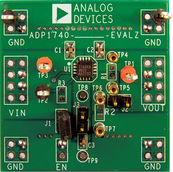
ADP1741 Evaluation Board
資料


AD9625 Evaluation and Synchronization
資料
ソフトウェア
リファレンス・デザイン


堅牢な、6 V ~14 V入力、多電圧、高効率、25Wユニバーサル電源モジュール ※Rev.0を翻訳したものです。新ver.は英語資料をご覧ください。