LTC3633A
LTC3633A-1
製造中
デュアル・チャネル、3A、20Vモノリシック同期整流式降圧レギュレータ
- 製品モデル
- 16
- 1Ku当たりの価格
- 最低価格:$5.07
製品の詳細
- 入力電圧範囲:3.6V~20V
- 出力電流:3A/チャネル
- 効率:最大95%
- 低デューティ・サイクル動作:5%(2.25MHz)
- チャネル間の位相偏移を選択可能:0°/180°
- 調整可能なスイッチング周波数:500kHz~4MHz
- 外部の周波数に同期
- 電流モード動作により、優れた入力および負荷トランジェント応答を実現
- 0.6Vのリファレンスにより、低出力電圧が可能
- Burst Mode®動作または強制連続動作をユーザーが選択可能
- 出力電圧トラッキング機能とソフトスタート機能
- 短絡保護
- 過電圧入力保護と過熱保護
- パワーグッド状態出力
- LTC3633:入力電圧の絶対最大定格が16V
- LTC3633A:20V絶対最大定格VIN、LTC3633とピン互換
- ロープロファイル(4mm × 5mm)QFN-28および28ピンTSSOPパッケージ
LTC3633Aは、デュアル・チャネルの高効率モノリシック同期整流式降圧レギュレータで、オン時間制御の電流モード・アーキテクチャを採用しており、スイッチング周波数の位相同期が可能です。2つのチャネルは位相を180°ずらして動作できるので、入力容量と出力容量の要件が緩和されます。動作電源電圧範囲は3.6V~20Vなので、リチウムイオン・バッテリ・スタックや12Vまたは5V電源を使用するポイントオブロード電源アプリケーションに最適です。
動作周波数は外付け抵抗を使用して500kHz~4MHzの範囲で設定可能で、外部クロック信号に同期させることもできます。高い周波数に対応できるので、小型の表面実装インダクタおよびコンデンサを使用できます。独自の固定周波数/オン時間制御アーキテクチャは、高周波で動作しながら高速トランジェント応答を必要とする高降圧比アプリケーションに最適です。内部の位相同期ループにより、内部ワンショット・タイマのオン時間をサーボ制御して、内部クロックまたは印加された外部クロックの周波数に合わせます。
LTC3633Aでは、強制連続モードと高効率のBurst Mode動作のいずれかを選択できます。LTC3633AとLTC3633A-1の違いは、出力電圧の検出範囲です(LTC3633A製品ファミリ全体の説明については、「動作」セクションの表1を参照してください)。
| Part Number | Output Voltage Sense Range | SVin Input | V2P5 Output | LTC3633 Pin Compatible |
| LTC3633A | 0.6V TO 6V | No | Yes | Yes |
| LTC3633A-1 | 1.5V TO 12V | No | Yes | Yes |
| LTC3633A-2 | 0.6V TO 6V | Yes | No | No |
| LTC3633A-3 | 1.5V TO 12V | Yes | No | No |
アプリケーション
- 分散給電システム
- バッテリ駆動計測器
- ポイントオブロード電源
ドキュメント
データシート 2
信頼性データ 1
ユーザ・ガイド 1
| 製品モデル | ピン/パッケージ図 | 資料 | CADシンボル、フットプリント、および3Dモデル |
|---|---|---|---|
| LTC3633AEFE#PBF | 28-Lead TSSOP w/ EP | ||
| LTC3633AEFE#TRPBF | 28-Lead TSSOP w/ EP | ||
| LTC3633AEFE-1#PBF | 28-Lead TSSOP w/ EP | ||
| LTC3633AEFE-1#TRPBF | 28-Lead TSSOP w/ EP | ||
| LTC3633AEUFD#PBF | 28-Lead QFN (4mm x 5mm x 0.75mm w/ EP) | ||
| LTC3633AEUFD#TRPBF | 28-Lead QFN (4mm x 5mm x 0.75mm w/ EP) | ||
| LTC3633AEUFD-1#PBF | 28-Lead QFN (4mm x 5mm x 0.75mm w/ EP) | ||
| LTC3633AEUFD-1#TRPBF | 28-Lead QFN (4mm x 5mm x 0.75mm w/ EP) | ||
| LTC3633AIFE#PBF | 28-Lead TSSOP w/ EP | ||
| LTC3633AIFE#TRPBF | 28-Lead TSSOP w/ EP | ||
| LTC3633AIFE-1#PBF | 28-Lead TSSOP w/ EP | ||
| LTC3633AIFE-1#TRPBF | 28-Lead TSSOP w/ EP | ||
| LTC3633AIUFD#PBF | 28-Lead QFN (4mm x 5mm x 0.75mm w/ EP) | ||
| LTC3633AIUFD#TRPBF | 28-Lead QFN (4mm x 5mm x 0.75mm w/ EP) | ||
| LTC3633AIUFD-1#PBF | 28-Lead QFN (4mm x 5mm x 0.75mm w/ EP) | ||
| LTC3633AIUFD-1#TRPBF | 28-Lead QFN (4mm x 5mm x 0.75mm w/ EP) |
| 製品モデル | 製品ライフサイクル | PCN |
|---|---|---|
|
4 6, 2022 - 22_0068 Laser Top Mark for ETSSOP and TSSOP Packages Assembled in ADPG [PNG] and UTL |
||
| LTC3633AEFE#PBF | 製造中 | |
| LTC3633AEFE#TRPBF | 製造中 | |
| LTC3633AEFE-1#PBF | 製造中 | |
| LTC3633AEFE-1#TRPBF | 製造中 | |
| LTC3633AIFE#PBF | 製造中 | |
| LTC3633AIFE#TRPBF | 製造中 | |
| LTC3633AIFE-1#PBF | 製造中 | |
| LTC3633AIFE-1#TRPBF | 製造中 | |
これは最新改訂バージョンのデータシートです。
ハードウェア・エコシステム
| 製品モデル | 製品ライフサイクル | 詳細 |
|---|---|---|
| デジタル・パワー・システム・マネージメント(PSM) 1 | ||
| LTC2977 | 新規設計に推奨 | 正確な出力電圧測定を特長とする8チャネルPMBusパワーシステム・マネージャ |
| 複数出力降圧レギュレータ 1 | ||
| LTC3633A-2 | 製造中 | デュアル・チャネル、3A、20Vモノリシック同期整流式降圧レギュレータ |
ツールおよびシミュレーション
LTspice 2
- LTC3633A - Step-Down (Buck) Regulators
- LTC3633A Demo Circuit - Dual Monolithic Synchronous Buck Regulator with LDO (3.6-20V to 1.8V/3.3V @ 3A & 2.5V @ 10mA)
下記製品はLTspiceで使用することが出来ます。:
- LTC3633
- LTC3633A
- LTC3633A-1
- LTC3633A-2
- LTC3633A-3
LTpowerCAD 2
LTspice®は、無料で提供される強力で高速な回路シミュレータと回路図入力、波形ビューワに改善を加え、アナログ回路のシミュレーションを容易にするためのモデルを搭載しています。
LTpowerCAD®は、電力段のデバイスの選択、詳細な電力効率の提供、ループのボーデ線図の安定性および負荷過渡応答解析の敏速な表示などを行うと共に、シミュレーション用にLTspiceにエクスポートできる電源設計プログラムです。
評価用キット
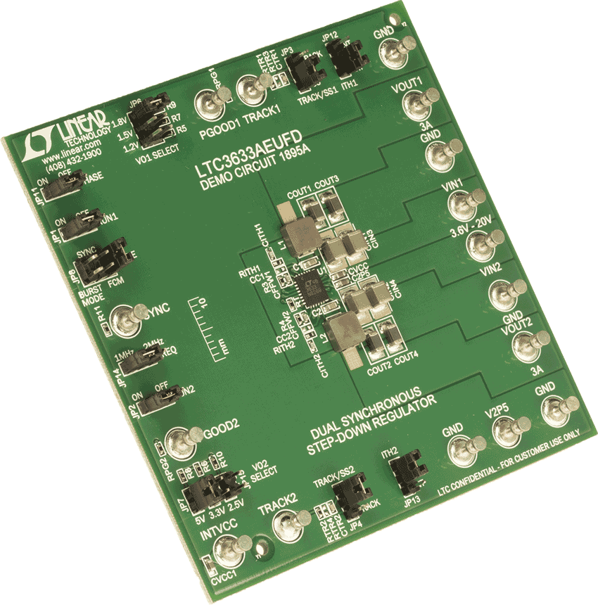
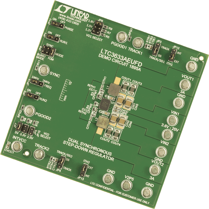
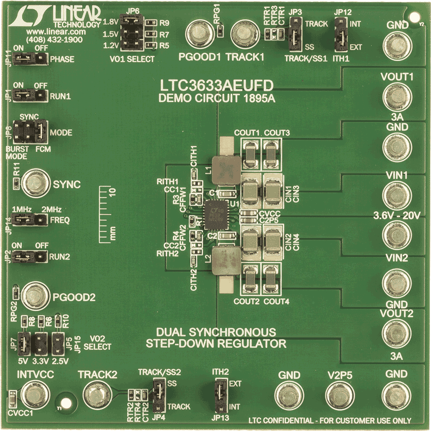
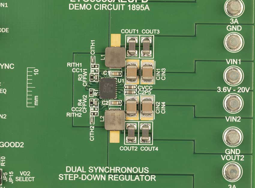
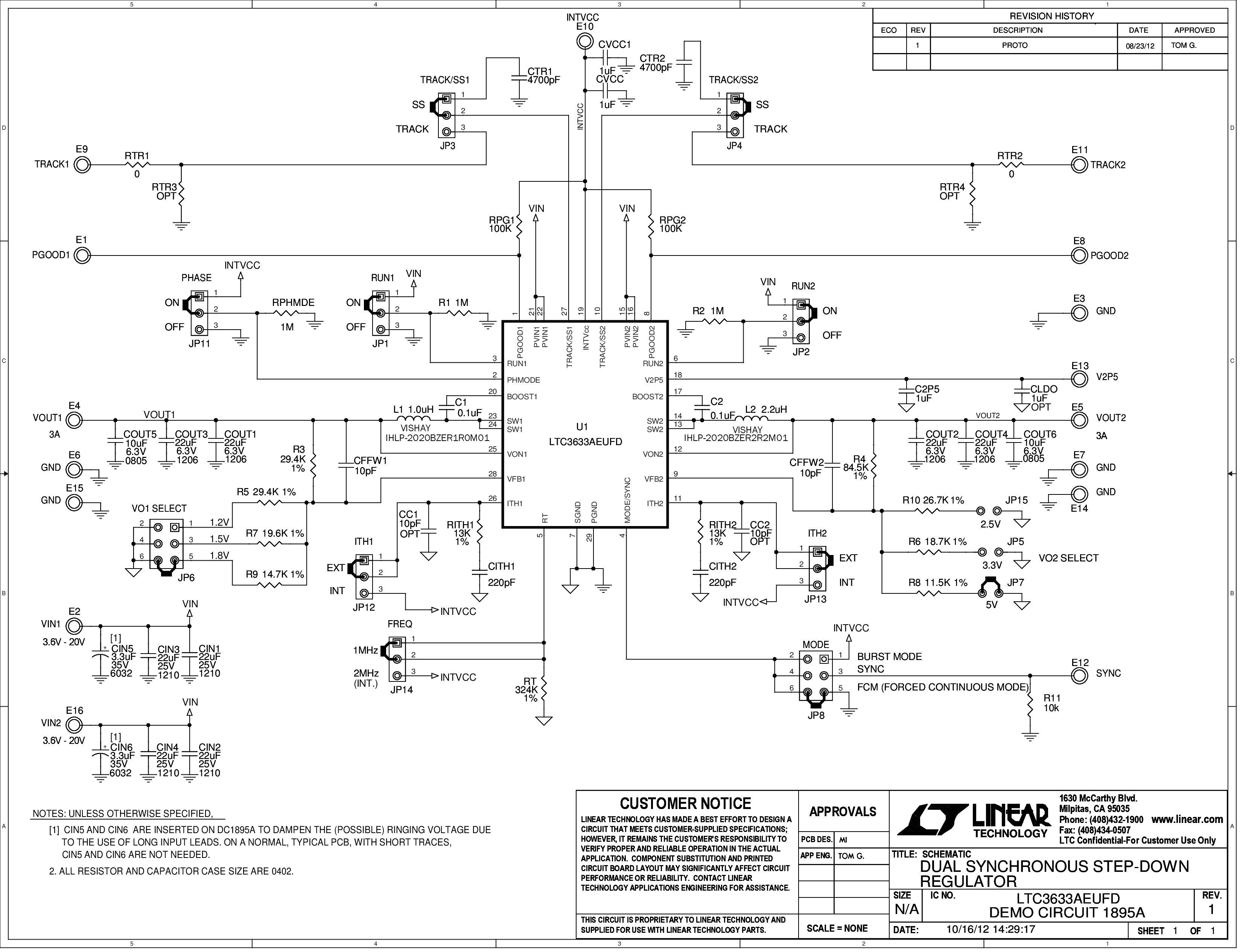
LTC3633AEUFD Demo Board | Dual Buck, 3.6V ≤ VIN ≤ 20V, VOUT1 = 1.2V/1.5V1.8V @ 3A, VOUT2 = 2.5V/3.3V/5V @ 3A
資料
リファレンス・デザイン
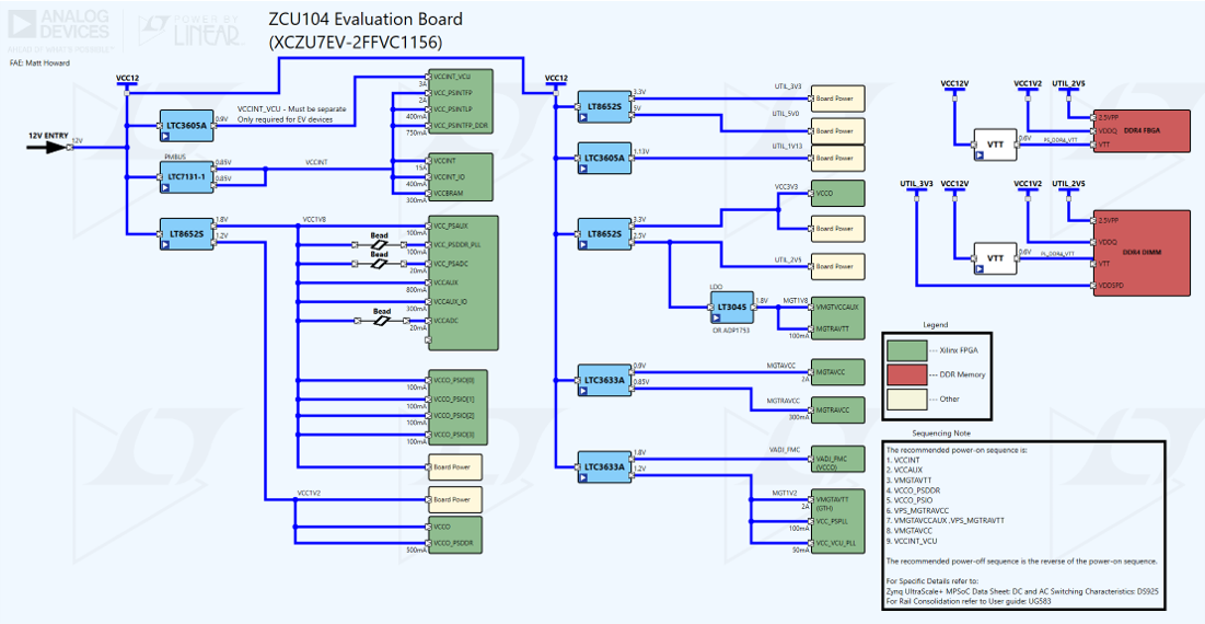
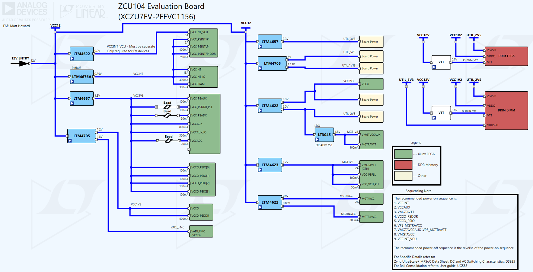
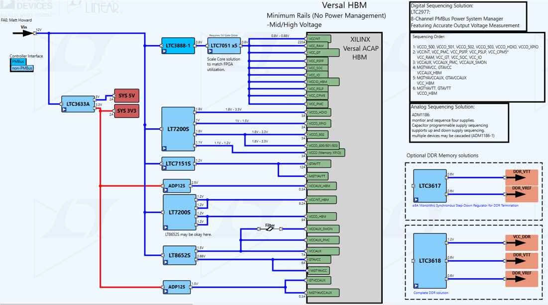
Zynq UltraScale+ MPSoC ZCU104 Paper Reference Design
使用製品