ADP1753
ADP1753
製造中ロー・ドロップアウト・レギュレータ(LDO)、調整機能付、800mA、低入力電圧
- 製品モデル
- 1
- 1Ku当たりの価格
- 最低価格:$1.20
Viewing:
製品の詳細
- 最大出力電流:0.8A
- 入力電圧範囲:1.6V~3.6V
- 低いシャットダウン電流:2μA未満
- 非常に低いドロップアウト電圧:70mV@0.8A負荷
- 初期精度:±1%
- ライン、負荷および温度にわたる:±2%
- ソフト・スタート機能つき7種の固定出力電圧オプション(ADP1752):0.75V~2.5V
- ソフト・スタート機能つき出力電圧調整可能オプション(ADP1753):0.75V~2.5V
- 高いPSRR性能(詳細はデータシートを参照して下さい。)
- 0.75V出力で23μV rms
- 小型4.7μFセラミック出力コンデンサで安定
- 優れた負荷およびラインのトランジエント応答特性
ADP1752 / ADP1753は、CMOS、ロー・ドロップアウト(LDO)リニア・レギュレータで、入力電圧は1.6V~3.6Vで動作し、出力電流は最大800mAまで供給することができます。
製品の詳細は電源構成の簡素化を実現するADP1740/41, ADP1752-1755をご覧ください。
このように低いVIN / VOUTを備えたLDOは、2.5Vから下の1.8V I/Oレールで動作し、0.75V以下のコア電圧に供給するナノメータ形状のFPGA用のレギュレータとして最適です。斬新で独自のアーキテクチャを使用することで、高い供給電圧除去、低ノイズを実現し、小型4.7μFのセラミック出力コンデンサとともに、優れたラインおよび負荷トランジエント応答を達成します。ADP1752には7種の固定出力電圧オプションがあります。ADP1753は、調整可能バージョンで、出力電圧は、外付けのデバイダによって、0.75V~3.0Vの範囲が可能です。ADP1752 / ADP1753は、外付けソフト・スタート・コンデンサを接続ずることによって、スタートアップをプログラムできます。パワーグッド出力は、パワー・システムモニタが、出力電源レール電圧の健全性をデジタル的にチェックします。
ADP1752 / ADP1753は、16ピンの4mm×4mm LFCSPパッケージで供給され、非常にコンパクトなソリューソンを実現できるだけではなく、小型、少フート・プリントで800mAの出力電流を必要とするアプリケーションに関して優れた熱性能を提供します。
ドキュメント
データシート 1
アプリケーション・ノート 2
技術記事 1
評価用設計ファイル 1
ビデオ 1

ソリューション・カタログ 2
Analog Dialogue 2
| 製品モデル | ピン/パッケージ図 | 資料 | CADシンボル、フットプリント、および3Dモデル |
|---|---|---|---|
| ADP1753ACPZ-R7 | 16-Lead LFCSP (4mm x 4mm w/ EP) |
| 製品モデル | 製品ライフサイクル | PCN |
|---|---|---|
|
5 5, 2014 - 14_0020 Conversion of 4x4mm body Size LFCSP Package Outlines from Punch to Sawn and Transfer of Assembly Site to Amkor Philippines. |
||
| ADP1753ACPZ-R7 | 製造中 | |
|
11 8, 2012 - 12_0290 ADP1740/ADP1741, ADP1752/ADP1753, ADP1754/ADP1755 Data Sheet Correction |
||
| ADP1753ACPZ-R7 | 製造中 | |
これは最新改訂バージョンのデータシートです。
ソフトウェア・リソース
必要なソフトウェア/ドライバが見つかりませんか?
ドライバ/ソフトウェアをリクエストハードウェア・エコシステム
| 製品モデル | 製品ライフサイクル | 詳細 |
|---|---|---|
| ADP1752 | 製造中 | ロー・ドロップアウト・レギュレータ(LDO)、800mA、低入力電圧 |
評価用キット


High speed data acquisition FMC board
資料
ソフトウェア


ADL5567 & AD9625 Analog Signal Chain Evaluation and ADF4355-2 Wideband Synthesizer with VCO
資料


ADA4961 & AD9625 Analog Signal Chain Evaluation and Converter Synchronization
資料
ソフトウェア
ADP1753 Evaluation Board
資料


AD9625 Evaluation and Synchronization
資料
ソフトウェア
リファレンス・デザイン
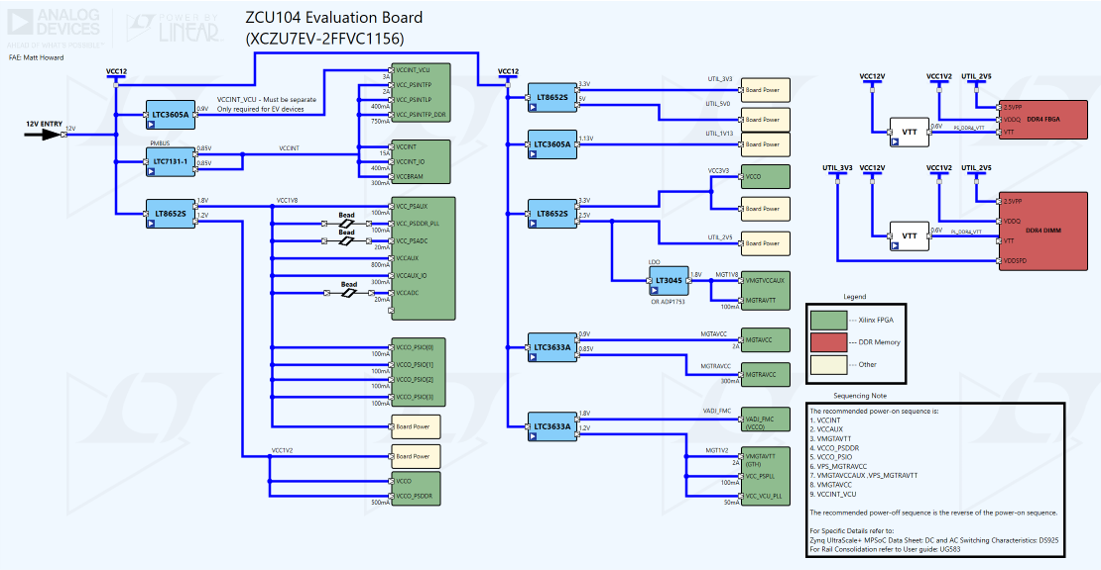
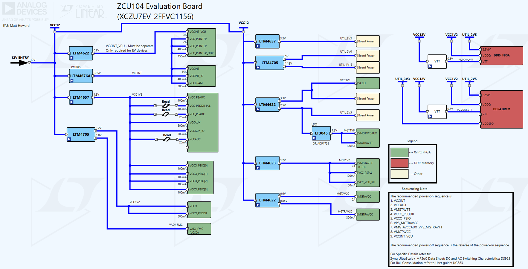
Zynq UltraScale+ MPSoC ZCU104 Paper Reference Design