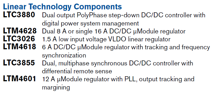
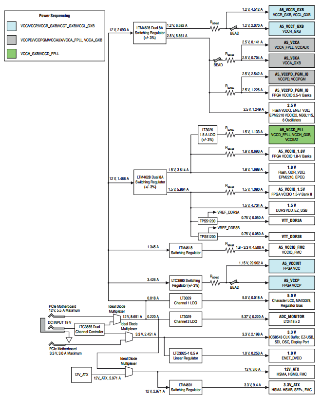
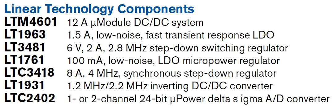
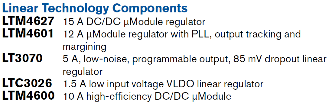
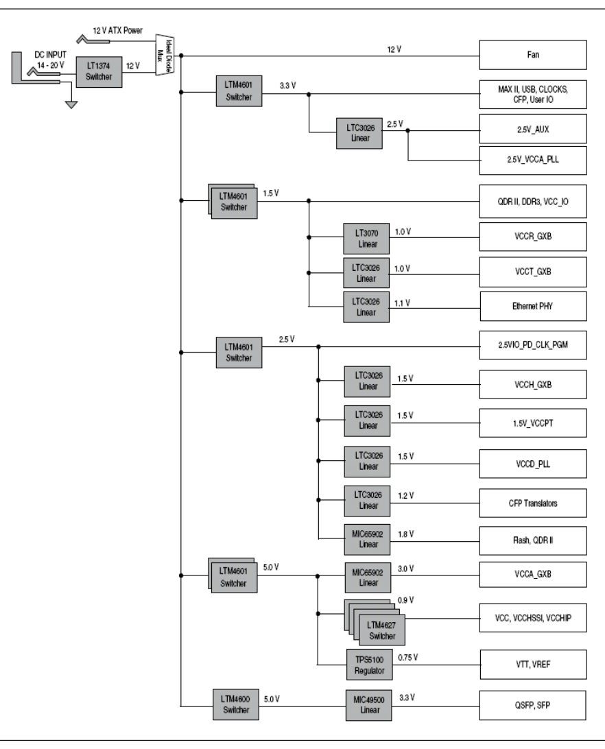
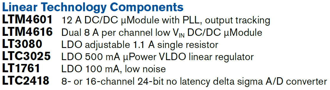
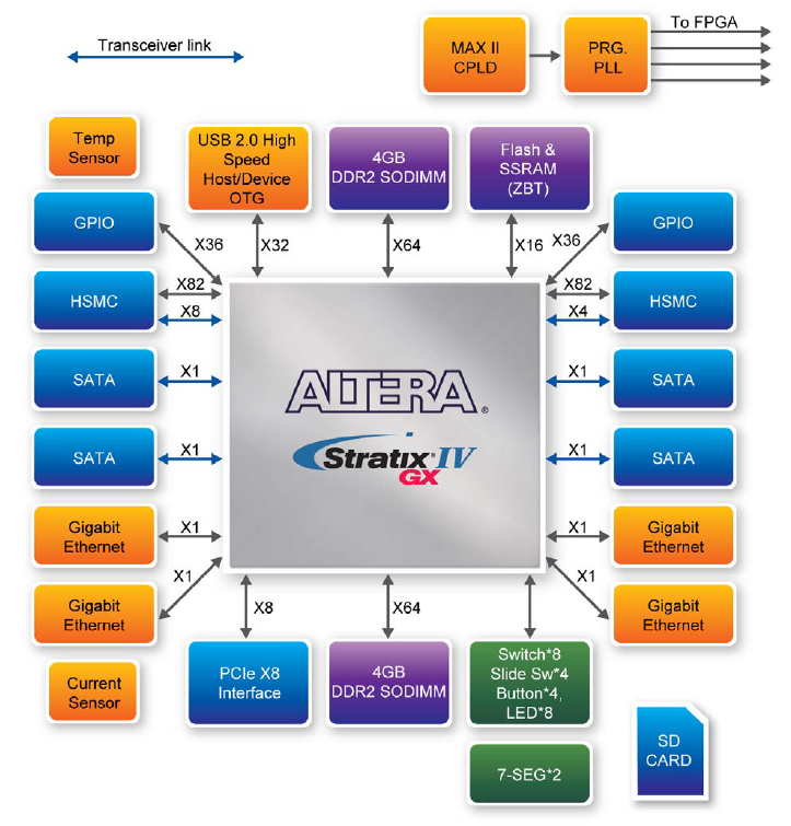
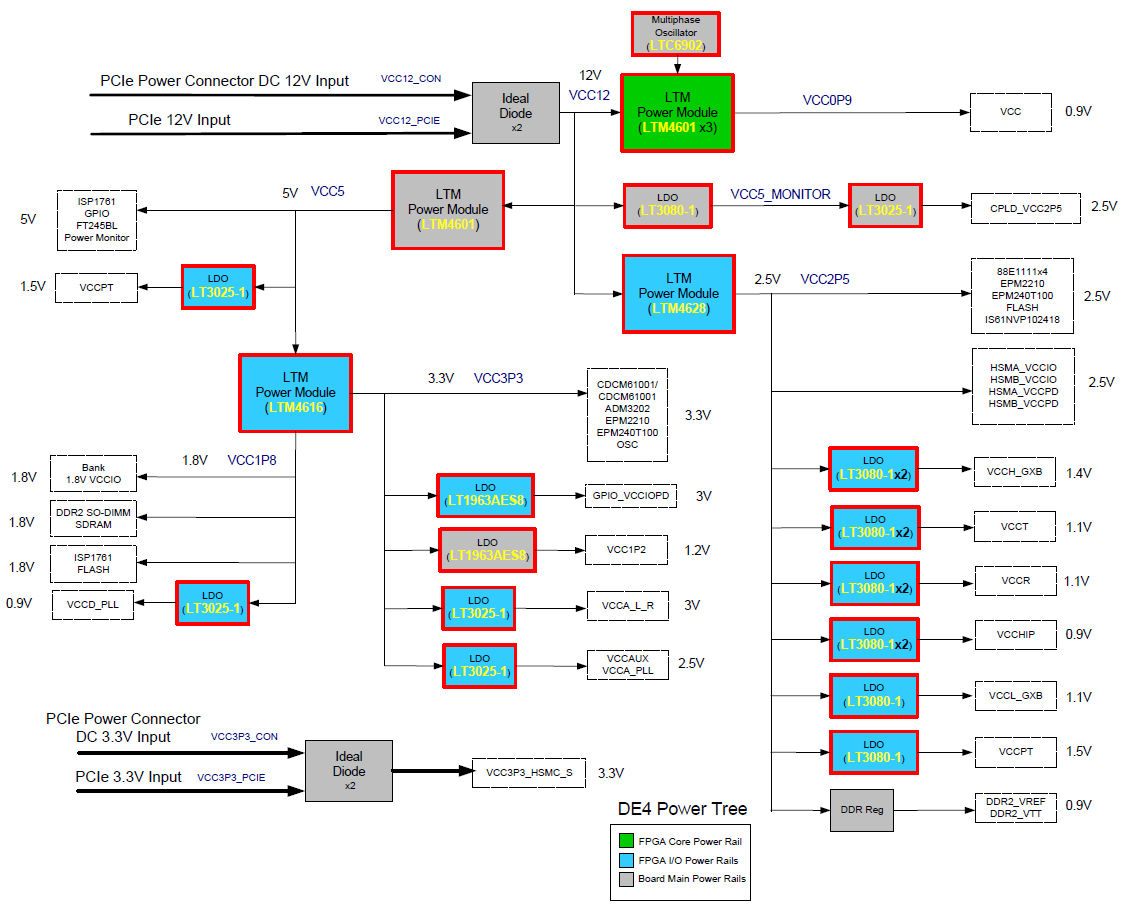
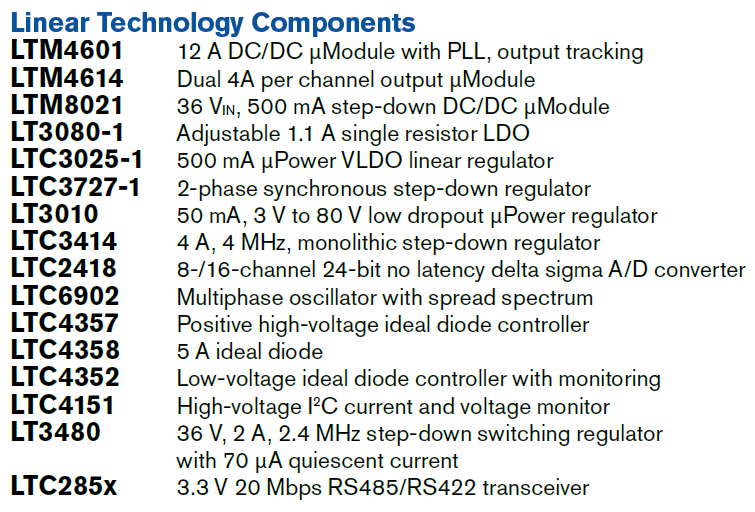
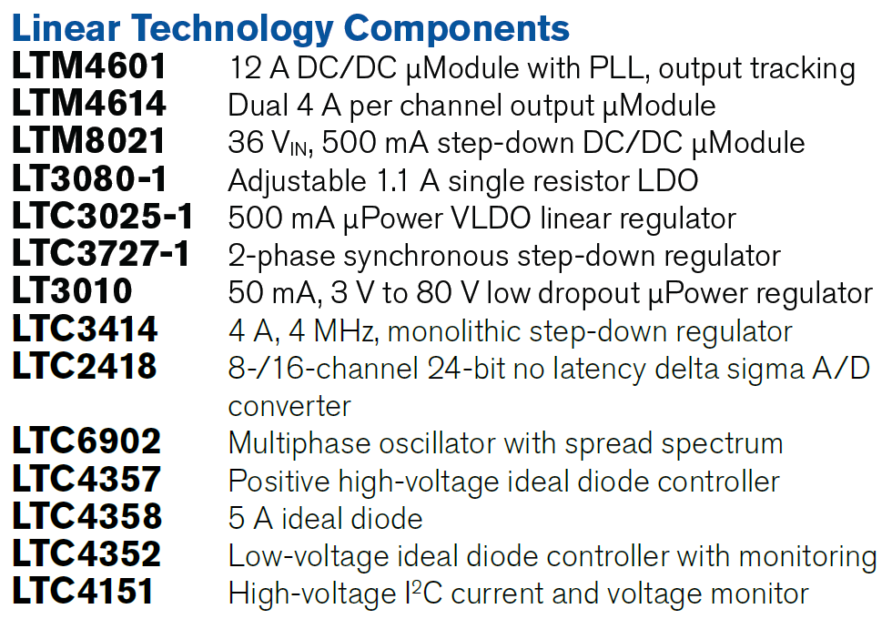
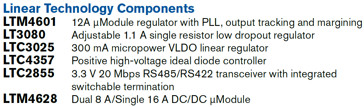
LTM4601

製造中

PLL、出力トラッキングおよびマージニングを備えた12A µModuleレギュレータ

利用上の注意

本データシートの英語以外の言語への翻訳はユーザの便宜のために提供されるものであり、リビジョンが古い場合があります。最新の内容については、必ず最新の英語版をご参照ください。

なお、日本語版のデータシートは基本的に「Rev.0」(リビジョン0)で作成されています。そのため、英語版が後に改訂され、複数製品のデータシートがひとつに統一された場合、同じ「Rev.0」の日本語版のデータシートが異なる製品のデータシートとして表示されることがあります。たとえば、「ADM3307E」の場合、日本語データシートをクリックすると「ADM3311E」が表示されます。これは、英語版のデータシートが複数の製品で共有できるように1本化され、「ADM3307E/ADM3310E/ADM3311E/ADM3312E/ADM3315E」(Rev.J)と改訂されたからで、決して誤ってリンクが張られているわけではありません。和文化されたデータシートを少しでも有効に活用していただくためにこのような方法をとっておりますので、ご了解ください。

アナログ・デバイセズ社は、提供する情報が正確で信頼できるものであることを期していますが、その情報の利用に関して、あるいはその利用によって生じる第三者の特許やその他の権利の侵害に関して一切の責任を負いません。また、アナログ・デバイセズ社の特許または特許の権利の使用を明示的または暗示的に許諾するものでもありません。仕様は予告なしに変更する場合があります。本紙記載の商標および登録商標は、各社の所有に属します。

製品の詳細

  • 完全なスイッチ・モード電源
  • 広い入力電圧範囲:4.5V~20V
  • 出力電流:標準12A(DC)、14A(ピーク値)
  • 出力電圧範囲:0.6V~5V
  • 出力電圧トラッキングおよびマージニング
  • 複数のμModuleレギュレータを並列接続することにより、電流分担を実現
  • 差動リモート検出による高精度レギュレーション(LTM4601のみ)
  • PLL周波数同期
  • ±1.5%のレギュレーション
  • 電流フォールドバック保護(起動時はディスエーブル)
  • SnPb仕上げまたはRoHS準拠の仕上げ
  • 超高速(UltraFast)トランジェント応答
  • 電流モード制御
  • 5V入力、3.3V出力時の効率:最大95%
  • プログラム可能なソフトスタート
  • 出力過電圧保護
  • 表面実装面積が小さく、高さの低い(15mm × 15mm × 2.82mm)表面実装LGAパッケージと(15mm × 15mm × 3.42mm)BGAパッケージ
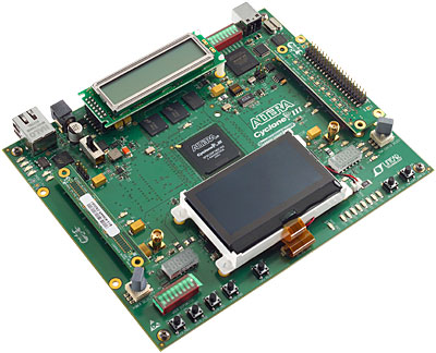
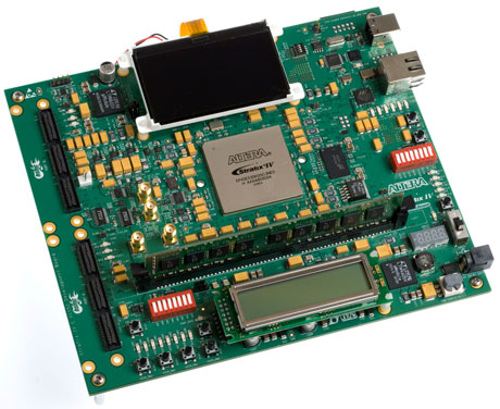
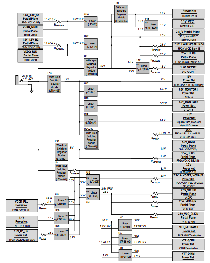
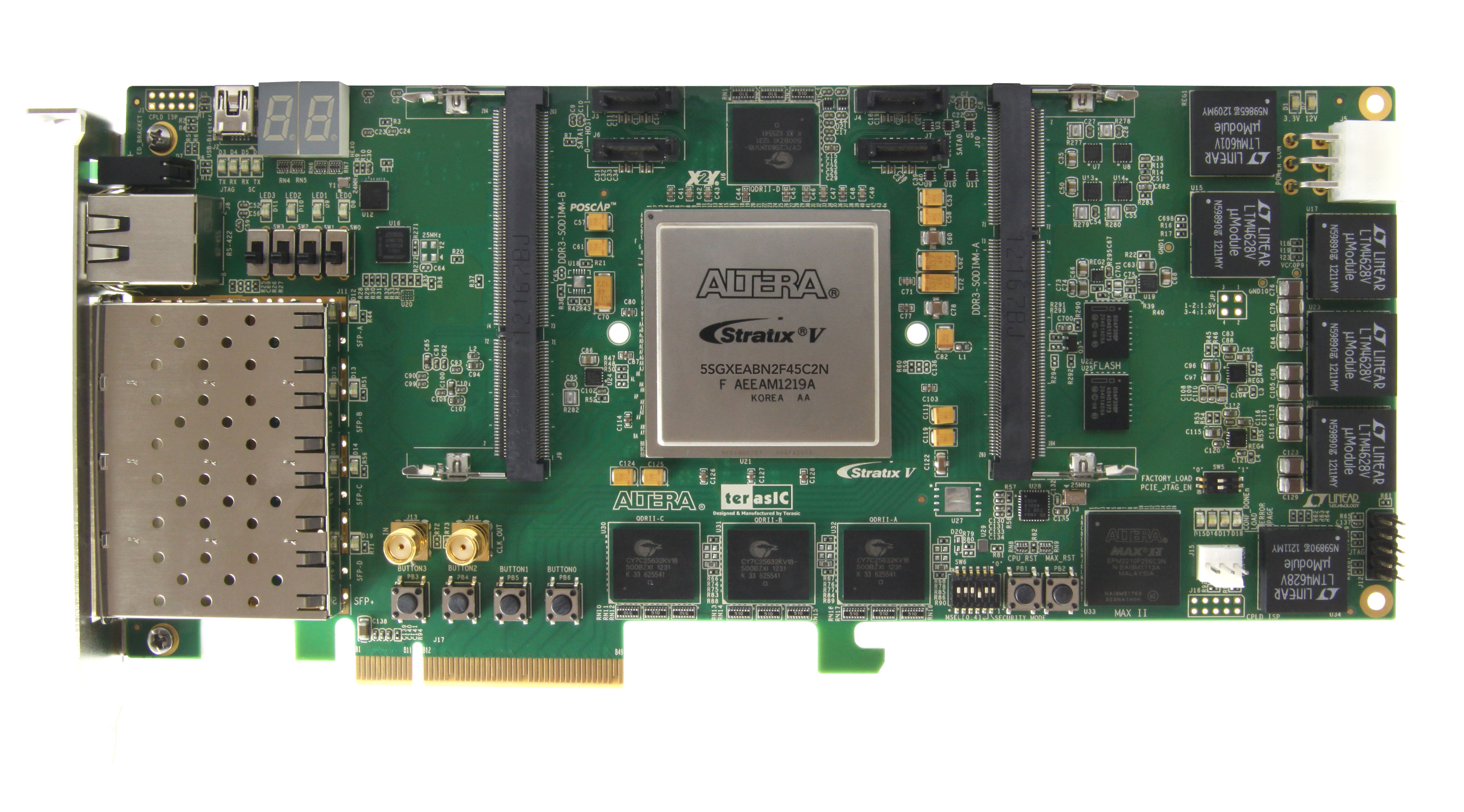
LTM4601
PLL、出力トラッキングおよびマージニングを備えた12A µModuleレギュレータ
質問する
サポート

アナログ・デバイセズのサポート・ページはアナログ・デバイセズへのあらゆるご質問にお答えするワンストップ・ポータルです。


ドキュメント

データシート

これは最新改訂バージョンのデータシートです。

さらに詳しく

ソフトウェア・リソース

必要なソフトウェア/ドライバが見つかりませんか?

ドライバ/ソフトウェアをリクエスト

ハードウェア・エコシステム

製品モデル 製品ライフサイクル 詳細
µModule 降圧レギュレータ 1
LTM4620A 製造中 デュアル13Aまたはシングル26A DC/DC μModuleレギュレータ
シリコン発振器 1
LTC6908 スペクトル拡散変調付き抵抗設定SOT-23発振器
デジタル・パワー・システム・マネージメント(PSM) 1
LTC2974 新規設計に推奨 正確な出力電流測定を特長とする4チャンネルPMBusパワーシステム・マネージャ
デュアル電源モニタ 1
LTC2960 新規設計に推奨 36Vナノ電流2入力電圧モニタ
高電圧ホットスワップ・コントローラ 1
LTC4364 新規設計に推奨 理想ダイオードを備えたサージ・ストッパー
Modal heading
myAnalogに追加

myAnalogの製品セクション(通知受け取り)、既存/新規プロジェクトに製品を追加する。

新規プロジェクトを作成

ツールおよびシミュレーション

LTspice

LTspice®は、無料で提供される強力で高速な回路シミュレータと回路図入力、波形ビューワに改善を加え、アナログ回路のシミュレーションを容易にするためのモデルを搭載しています。


評価用キット

eval board
DC1118A-A

LTM4601EV Demo Board | LTM4601(x2), 5V ≤ VIN ≤ 20V, VOUT1 = 3.3V @ 10A, VOUT2 = 2.5V @ 12A

製品詳細

Demonstration circuit 1118A-A features two independent LTM4601EV high efficiency, high density switch mode step-down power modules. The input voltage range is from 5V to 20V. The output voltages are 3.3V and 2.5V; refer to step down ratio curve in the LTM4601 datasheet. The rated load currents are 10A for the 3.3V output and 12A for the 2.5V output, while derating is necessary for certain VIN and thermal conditions. The output of U2 is set to coincidentally track with the 3.3V output. Margining function is provided for the user who wants to stress their system by varying supply voltages during testing. Integrated input and output filters enable a simple PCB layout. Only bulk input and output capacitors are needed.


eval board
DC1041A-A

LTM4601 Demo Board | 4.5V ≤ VIN ≤ 20V, VOUT = 0.6V to 5V @ 12A

製品詳細

Demonstration circuit DC1041A-A features the LTM4601EV, a 12A high efficiency, high density switch mode step-down converter. The input voltage range is from 4.5V to 20V. The output voltage is jumper selectable for popular voltages from 0.6V to 5V. The PLLIN pin supports synchronizing the μModule® regulator to an external clock. The TRACK/SS pin allows the user to program output ramp-up and ramp-down rates which may coincidentally or ratiometrically track with another supply’s output if desired. Output voltage margining of ±5% from the nominal value is available via the margin control pins MARG0 and MARG1.

eval board
DC1043A-C

LTM4601 Demo Board | LTM4601(×4), 5V ≤ VIN ≤ 20V, VOUT = 0.6V to 3.3V @ 40A

製品詳細

Demonstration circuit DC1043A-C features four LTM4601EV high efficiency, high density switch mode step-down power modules in parallel (the LTM4601-1 can be substituted for the slave devices). The input voltage range is from 5.0V to 20V. The output voltage is programmable from 0.6V to 3.3V; refer to step down ratio curve in the LTM4601 datasheet. The rated load current is 40A, while de-rating is necessary for certain VIN, VOUT, and thermal conditions. Master module U1 provides differential remote sensing to accurately regulate output voltage independent of load current. Integrated input and output filters enable a simple PCB layout. Only bulk input and output capacitors are needed externally.

eval board
DC1118A-C

LTM4601EV Demo Board | LTM4601(x4), 5V ≤ VIN ≤ 20V, VOUT1 = 3.3V @ 10A, VOUT2 = 2.5V @ 12A, VOUT3 = 1.8V @ 12A, VOUT4 = 1.5V @ 12A

製品詳細

Demonstration circuit 1118A-C features four independent LTM4601EV high efficiency, high density switch mode step-down power modules. The input voltage range is from 5V to 20V. The output voltages are 3.3V, 2.5V,1.8V and 1.5V; refer to step down ratio curve in the LTM4601 datasheet. The rated load currents are 10A for the 3.3V output, and 12A for the 2.5V, 1.8V and 1.5V outputs, while derating is necessary for certain VIN and thermal conditions. The output of U2 is set to coincidentally track with the 3.3V output. Margining function is provided for the user who wants to stress their system by varying supply voltages during testing. Integrated input and output filters enable a simple PCB layout; only bulk input and output capacitors are needed.


eval board
DC1118A-B

LTM4601EV Demo Board | LTM4601(x3), 5V ≤ VIN ≤ 20V, VOUT1 = 3.3V @ 10A, VOUT2 = 2.5V @ 12A, VOUT3 = 1.8V @ 12A

製品詳細

Demonstration circuit 1118A-B features three independent LTM4601EV high efficiency, high density switch mode step-down power modules. The input voltage range is from 5V to 20V. The output voltages are 3.3V, 2.5V and 1.8V; refer to step down ratio curve in the LTM4601 datasheet. The rated load currents are 10A for the 3.3V output, 12A for the 2.5V output and 12A for the 1.8V output, while derating is necessary for certain VIN and thermal conditions. The output of U2 is set to coincidentally track with the 3.3V output. Margining function is provided for the user who wants to stress their system by varying supply voltages during testing. Integrated input and output filters enable a simple PCB layout; only bulk input and output capacitors are needed.

eval board
DC1043A-B

LTM4601 Demo Board | LTM4601(×3), 5V ≤ VIN ≤ 20V, VOUT = 0.6V to 3.3V @ 30A

製品詳細

Demonstration circuit DC1043A-B features three LTM4601EV high efficiency, high density switch mode step-down power modules in parallel (the LTM4601-1 can be substituted for the slave devices). The input voltage range is from 5.0V to 20V. The output voltage is programmable from 0.6V to 3.3V; refer to step down ratio curve in the LTM4601 datasheet. The rated load current is 30A, while de-rating is necessary for certain VIN, VOUT, and thermal conditions. Master module U1 provides differential remote sensing to accurately regulate output voltage independent of load current. Integrated input and output filters enable a simple PCB layout. Only bulk input and output capacitors are needed externally.

eval board
DC1043A-A

LTM4601 Demo Board | LTM4601(×2), 5V ≤ VIN ≤ 20V, VOUT = 0.6V to 3.3V @ 20A

製品詳細

Demonstration circuit DC1043A-A features the LTM4601EV and LTM4601-1EV, the high efficiency, high density switch mode step-down power modules. The input voltage range is from 5.0V to 20V. The output voltage is programmable from 0.6V to 3.3V; refer to step down ratio curve in the LTM4601 datasheet. The rated load current is 20A, while de-rating is necessary for certain VIN, VOUT, and thermal conditions. 24A load current can be achieved by applying forced airflow convection or attaching heatsinks. Master module U1 provides differential remote sensing to accurately regulate output voltage independent of load current. Integrated input and output filters enable a simple PCB layout. Only bulk input and output capacitors are needed externally. The DC1043A-A has on-board 180 degree interleaving clock generator.

DC1118A-A
LTM4601EV Demo Board | LTM4601(x2), 5V ≤ VIN ≤ 20V, VOUT1 = 3.3V @ 10A, VOUT2 = 2.5V @ 12A
DC1041A-A
LTM4601 Demo Board | 4.5V ≤ VIN ≤ 20V, VOUT = 0.6V to 5V @ 12A
DC1043A-C
LTM4601 Demo Board | LTM4601(×4), 5V ≤ VIN ≤ 20V, VOUT = 0.6V to 3.3V @ 40A
DC1118A-C
LTM4601EV Demo Board | LTM4601(x4), 5V ≤ VIN ≤ 20V, VOUT1 = 3.3V @ 10A, VOUT2 = 2.5V @ 12A, VOUT3 = 1.8V @ 12A, VOUT4 = 1.5V @ 12A
DC1118A-B
LTM4601EV Demo Board | LTM4601(x3), 5V ≤ VIN ≤ 20V, VOUT1 = 3.3V @ 10A, VOUT2 = 2.5V @ 12A, VOUT3 = 1.8V @ 12A
DC1043A-B
LTM4601 Demo Board | LTM4601(×3), 5V ≤ VIN ≤ 20V, VOUT = 0.6V to 3.3V @ 30A
DC1043A-A
LTM4601 Demo Board | LTM4601(×2), 5V ≤ VIN ≤ 20V, VOUT = 0.6V to 3.3V @ 20A

リファレンス・デザイン

DK-EMB-3C120N Dev Kit
Altera Embedded Systems Development Kit, Cyclone III Edition Circuits from the Lab®

機能と利点

  • Analog Devices has worked closely with FPGA and processor manufacturers to develop verified power solutions that optimize cost, size and efficiency in high performance applications
  • Our reference designs are supported by an intuitive design tool set and IP
  • Our team can provide designs for quick prototypes that can speed time to market in the most complex applications
DK-DEV-5AGTD7N Dev Kit
Altera Arria V GT FPGA Development Kit Circuits from the Lab®

機能と利点

  • Analog Devices has worked closely with FPGA and processor manufacturers to develop verified power solutions that optimize cost, size and efficiency in high performance applications
  • Our reference designs are supported by an intuitive design tool set and IP
  • Our team can provide designs for quick prototypes that can speed time to market in the most complex applications
DK-DEV-4SE530N Dev Kit
Altera Stratix IV E FPGA Development Kit Circuits from the Lab®

機能と利点

  • Analog Devices has worked closely with FPGA and processor manufacturers to develop verified power solutions that optimize cost, size and efficiency in high performance applications
  • Our reference designs are supported by an intuitive design tool set and IP
  • Our team can provide designs for quick prototypes that can speed time to market in the most complex applications
DK-DSP-3C120N Dev Kit
Altera DSP Development Kit, Cyclone III Edition Circuits from the Lab®

機能と利点

  • Analog Devices has worked closely with FPGA and processor manufacturers to develop verified power solutions that optimize cost, size and efficiency in high performance applications
  • Our reference designs are supported by an intuitive design tool set and IP
  • Our team can provide designs for quick prototypes that can speed time to market in the most complex applications
TR5-F40W Dev Kit
Terasic TR5-F40W Stratix V GX FPGA Development Kit Circuits from the Lab®

機能と利点

  • Analog Devices has worked closely with FPGA and processor manufacturers to develop verified power solutions that optimize cost, size and efficiency in high performance applications
  • Our reference designs are supported by an intuitive design tool set and IP
  • Our team can provide designs for quick prototypes that can speed time to market in the most complex applications
DK-100G-5SGXEA7N Dev Kit
Altera 100G Development Kit, Stratix V Edition Circuits from the Lab®

機能と利点

  • Analog Devices has worked closely with FPGA and processor manufacturers to develop verified power solutions that optimize cost, size and efficiency in high performance applications
  • Our reference designs are supported by an intuitive design tool set and IP
  • Our team can provide designs for quick prototypes that can speed time to market in the most complex applications
DK-SI-4SGX230N Kit
Altera Transceiver Signal Integrity Kit, Stratix IV GX Edition Circuits from the Lab®

機能と利点

  • Analog Devices has worked closely with FPGA and processor manufacturers to develop verified power solutions that optimize cost, size and efficiency in high performance applications
  • Our reference designs are supported by an intuitive design tool set and IP
  • Our team can provide designs for quick prototypes that can speed time to market in the most complex applications
DE4 Dev Kit
Terasic DE4 Development and Education Board Circuits from the Lab®

機能と利点

  • Analog Devices has worked closely with FPGA and processor manufacturers to develop verified power solutions that optimize cost, size and efficiency in high performance applications
  • Our reference designs are supported by an intuitive design tool set and IP
  • Our team can provide designs for quick prototypes that can speed time to market in the most complex applications
TR4 Stratix IV Board
Terasic TR4 Stratix IV Board Circuits from the Lab®

機能と利点

  • Analog Devices has worked closely with FPGA and processor manufacturers to develop verified power solutions that optimize cost, size and efficiency in high performance applications
  • Our reference designs are supported by an intuitive design tool set and IP
  • Our team can provide designs for quick prototypes that can speed time to market in the most complex applications
DK-VIDEO-4SGX230N Dev Kit
Altera Audio Video Development Kit, Stratix IV GX Edition Circuits from the Lab®

機能と利点

  • Analog Devices has worked closely with FPGA and processor manufacturers to develop verified power solutions that optimize cost, size and efficiency in high performance applications
  • Our reference designs are supported by an intuitive design tool set and IP
  • Our team can provide designs for quick prototypes that can speed time to market in the most complex applications
DK-DEV-4SGX230N Dev Kit
Altera Stratix IV GX FPGA Development Kit Circuits from the Lab®

機能と利点

  • Analog Devices has worked closely with FPGA and processor manufacturers to develop verified power solutions that optimize cost, size and efficiency in high performance applications
  • Our reference designs are supported by an intuitive design tool set and IP
  • Our team can provide designs for quick prototypes that can speed time to market in the most complex applications
DK-DEV-5AGXB3NES Dev Kit
Altera Arria V GX FPGA Development Kit Circuits from the Lab®

機能と利点

  • Analog Devices has worked closely with FPGA and processor manufacturers to develop verified power solutions that optimize cost, size and efficiency in high performance applications
  • Our reference designs are supported by an intuitive design tool set and IP
  • Our team can provide designs for quick prototypes that can speed time to market in the most complex applications
DE5-Net Dev Kit
Terasic DE5-Net Stratix V Board Circuits from the Lab®

機能と利点

  • Analog Devices has worked closely with FPGA and processor manufacturers to develop verified power solutions that optimize cost, size and efficiency in high performance applications
  • Our reference designs are supported by an intuitive design tool set and IP
  • Our team can provide designs for quick prototypes that can speed time to market in the most complex applications
DK-DEV-3C120N Dev Kit
Altera Cyclone III FPGA Development Kit Circuits from the Lab®

機能と利点

  • Analog Devices has worked closely with FPGA and processor manufacturers to develop verified power solutions that optimize cost, size and efficiency in high performance applications
  • Our reference designs are supported by an intuitive design tool set and IP
  • Our team can provide designs for quick prototypes that can speed time to market in the most complex applications
Altera Embedded Systems Development Kit, Cyclone III Edition
Altera Arria V GT FPGA Development Kit
Altera Stratix IV E FPGA Development Kit
Altera DSP Development Kit, Cyclone III Edition
Terasic TR5-F40W Stratix V GX FPGA Development Kit
Altera 100G Development Kit, Stratix V Edition
Altera Transceiver Signal Integrity Kit, Stratix IV GX Edition
Terasic DE4 Development and Education Board
Terasic TR4 Stratix IV Board
Altera Audio Video Development Kit, Stratix IV GX Edition
Altera Stratix IV GX FPGA Development Kit
Altera Arria V GX FPGA Development Kit
Terasic DE5-Net Stratix V Board
Altera Cyclone III FPGA Development Kit

最新のディスカッション

最近表示した製品