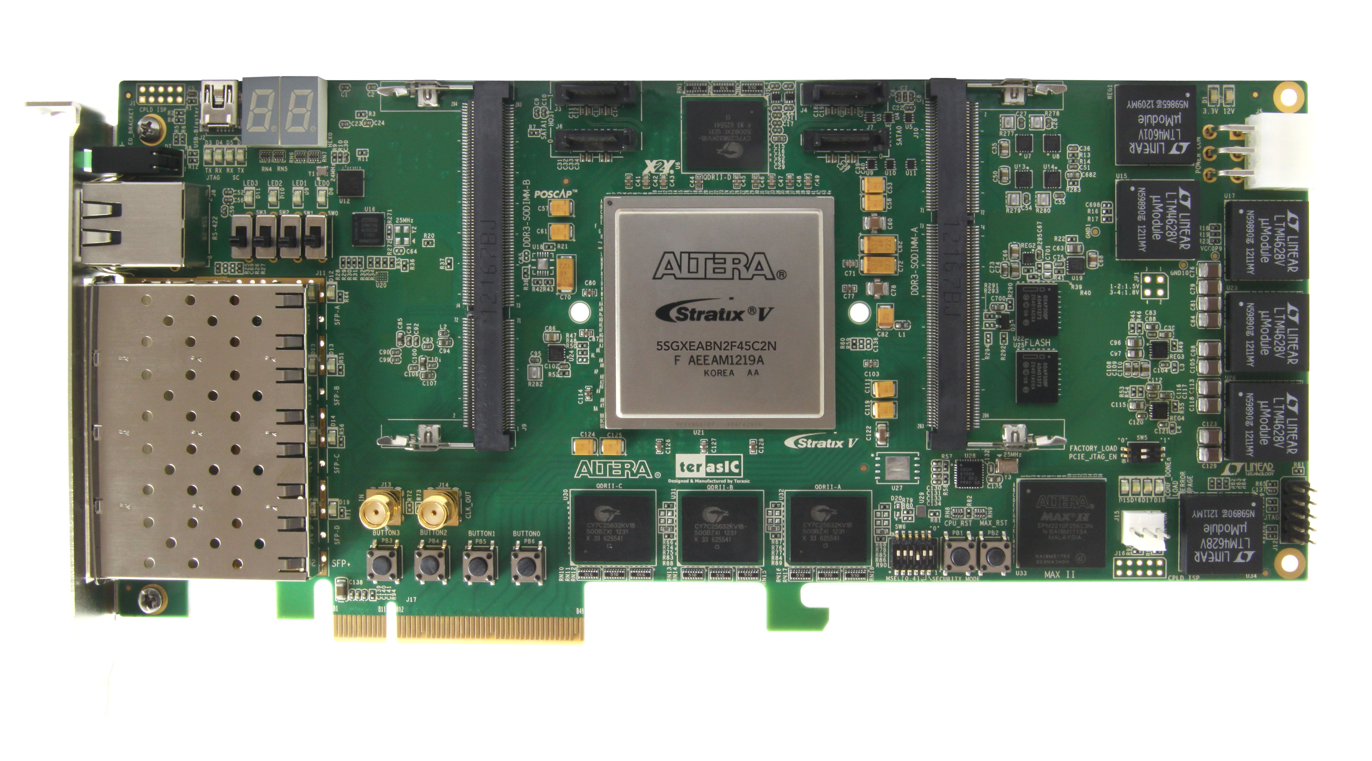
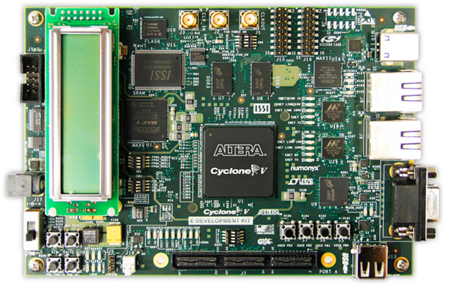
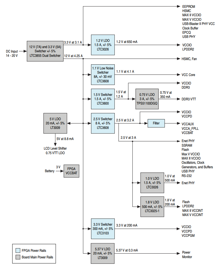
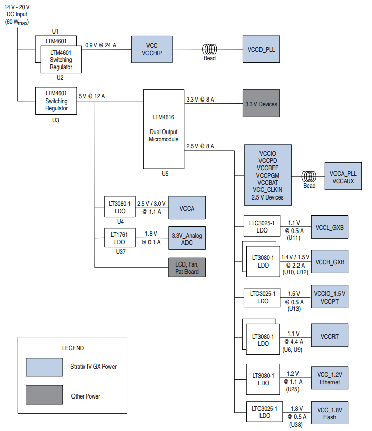
LTC3025
LTC3025
製造中300mA、マイクロパワー、VLDOリニア・レギュレータ
- 製品モデル
- 4
- 1Ku当たりの価格
- 最低価格:$1.66
Viewing:
製品の詳細
- 広い入力電圧範囲:0.9V~5.5V
- セラミック・コンデンサで安定
- 非常に低いドロップアウト: 300mAで45mV
- 調整可能な出力電圧範囲:0.4V~3.6V
- 温度、電源、負荷の全範囲で±2%の電圧精度
- 低ノイズ:80μVRMS(10Hz~100kHz)
- BIAS電圧範囲:2.5V~5.5V
- 高速過渡回復
- シャットダウン時にVINとVBIASから負荷を切断
- 低い動作電流:IIN = 4μA、IBIAS = 50μA(標準)
- 低いシャットダウン電流:IIN = 1μA、IBIAS = 0.01μA(標準)
- 出力電流制限
- 熱過負荷保護機能
- 6ピン(2mm×2mm)DFNパッケージ
LTC3025は、0.9Vという低い入力電圧で動作する、マイクロパワーVLDO™(超低損失)リニア・レギュレータです。標準わずか45mVの損失電圧で300mAの出力電流を供給可能です。高効率のレギュレーションを行うために出力電流がIN電源から直接供給されているので、内部リファレンスとLDO回路を動かすためにBIAS電源が必要です。内部リファレンス電圧が0.4Vと低いので、LTC3025の出力は一般的なLDOに比べてかなり低い電圧(0.4V~3.6V)にプログラムできます。出力電圧は2本の超小型SMD抵抗を介してプログラムされます。
低消費電流のLTC3025は、バッテリ駆動システムでの使用に最適です。3セルNiMHや1セル・リチウムイオンのアプリケーションにおいて、BIAS電圧はバッテリから直接供給可能で、入力は高効率の降圧レギュレータから得ることができるので、高効率で低ノイズの出力を供給します。
他の特長として、高い出力電圧精度、優れた過渡応答、1μFの超低ESRセラミック・コンデンサでの安定、短絡および熱過負荷保護、出力電流制限などがあります。 LTC3025は高さの低い(0.75mm)小型の6ピンDFN(2mm×2mm)パッケージで供給されます。
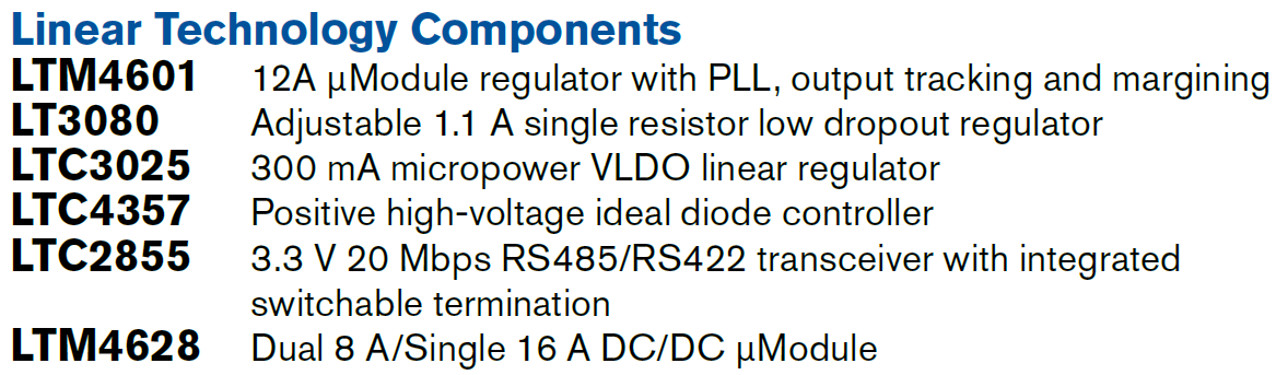
| Output Current | Output Voltage | |
| LTC3025 | 300mA | Adj (0.4V to 3.6V) |
| LTC3025-1 | 500mA | Adj (0.4V to 3.6V) |
| LTC3025-2 | 500mA | 1.2V Fixed |
| LTC3025-3 | 500mA | 1.5V Fixed |
| LTC3025-4 | 500mA | 1.8V Fixed |
- 低消費電力ハンドヘルド機器
- 低電圧ロジック電源
- DSP電源
- 携帯電話
- 携帯用電子機器
- ハンドヘルド医療機器
- スイッチング電源ノイズ除去用ポスト・レギュレータ
ドキュメント
データシート 2
信頼性データ 1
ユーザ・ガイド 1
アプリケーション・ノート 1
技術記事 1
ソリューション・カタログ 2
プレス・リリース 1
| 製品モデル | ピン/パッケージ図 | 資料 | CADシンボル、フットプリント、および3Dモデル |
|---|---|---|---|
| LTC3025EDC#TRMPBF | 6-Lead DFN (2mm x 2mm w/ EP) | ||
| LTC3025EDC#TRPBF | 6-Lead DFN (2mm x 2mm w/ EP) | ||
| LTC3025IDC#TRMPBF | 6-Lead DFN (2mm x 2mm w/ EP) | ||
| LTC3025IDC#TRPBF | 6-Lead DFN (2mm x 2mm w/ EP) |
これは最新改訂バージョンのデータシートです。
ソフトウェア・リソース
必要なソフトウェア/ドライバが見つかりませんか?
ドライバ/ソフトウェアをリクエストハードウェア・エコシステム
ツールおよびシミュレーション
LTspice 2
- LTC3025/LTC3406-1.5 Demo Circuit - High Efficiency Step-Down Converter with VLDO (2.7-5.5V to 1.5V @ 600mA & 1.2V @ 300mA)
- LTC3035/LTC3025 Demo Circuit - Dual LDO Output (1.7-5.5V to 1.5V/1.8V @ 300mA)
下記製品はLTspiceで使用することが出来ます。:
- LTC3025
- LTC3025-1
- LTC3025-2
- LTC3025-3
- LTC3025-4
LTspice®は、無料で提供される強力で高速な回路シミュレータと回路図入力、波形ビューワに改善を加え、アナログ回路のシミュレーションを容易にするためのモデルを搭載しています。
評価用キット

LTC3025EDC Demo Board | Low VIN, VLDO Line ar Regulator, 0.9V ≤ VIN ≤ 5.5V, VOUT = 0.8V/1.2V/1.5V/1.8V/Adj @ 300mA
資料
リファレンス・デザイン
使用製品
使用製品

使用製品