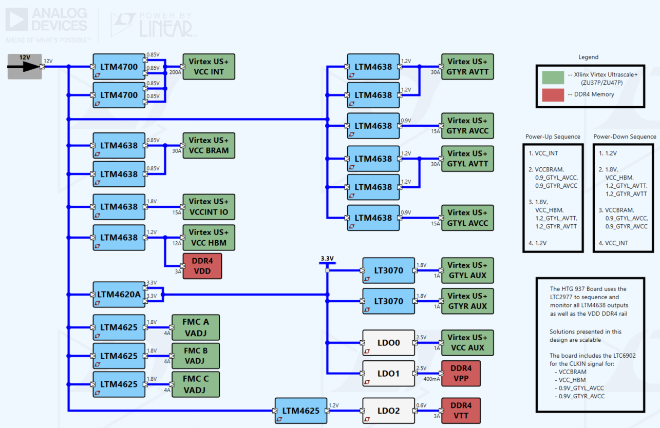
LTM4620A
製造中デュアル13Aまたはシングル26A DC/DC μModuleレギュレータ
- 製品モデル
- 7
- 1Ku当たりの価格
- 最低価格:$36.82
製品の詳細
- デュアル13A出力またはシングル26A出力
- 広い入力電圧範囲:4.5V~16V
- 出力電圧範囲:0.6V~5.3V
- 全DC出力電圧誤差:最大±1.5%
- 複数のLTM4620Aによるマルチフェーズ電流分担:最大100A
- LTM4620より高効率かつ出力電圧範囲が広い
- 差動リモート検出アンプ
- 電流モード制御/高速トランジェント応答
- 調整可能なスイッチング周波数
- 過電流フォールドバック保護
- 周波数同期
- 内部温度モニタ
- 出力過電圧保護
- LTM4628(デュアル8A)およびLTM4620(デュアル13A)とピン互換
- 熱特性が改善された(15mm × 15mm × 4.41mm)LGAパッケージおよび(15mm × 15mm × 5.01mm)BGAパッケージ
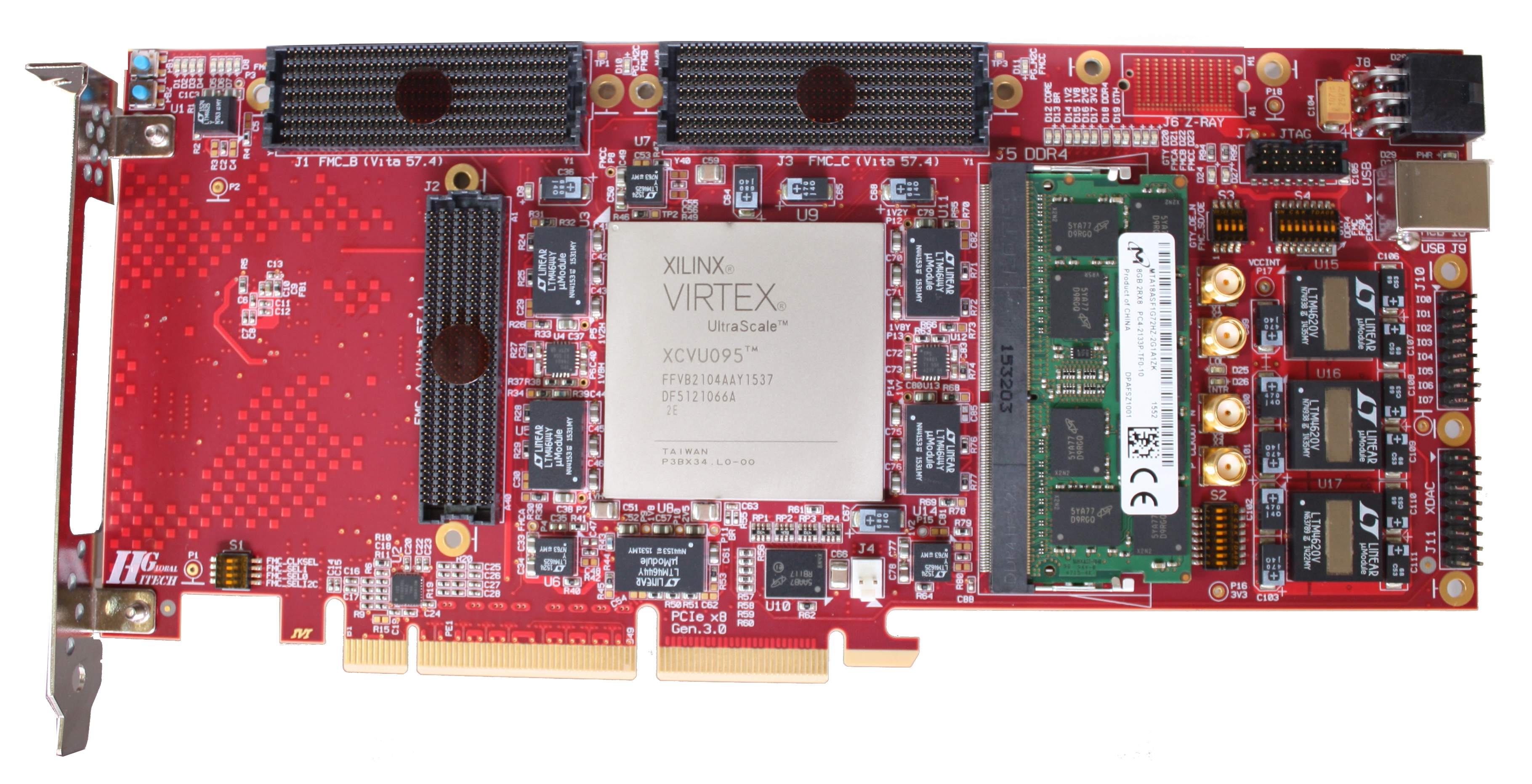
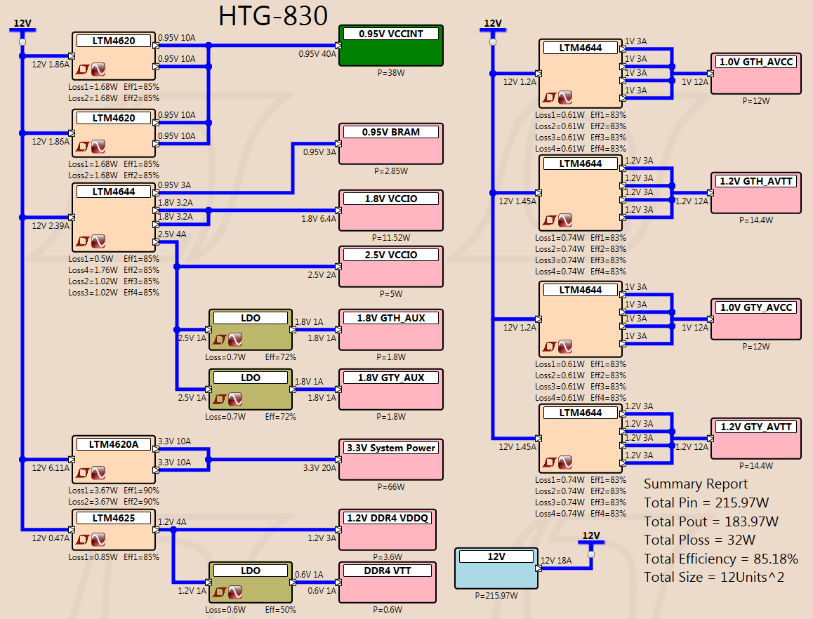
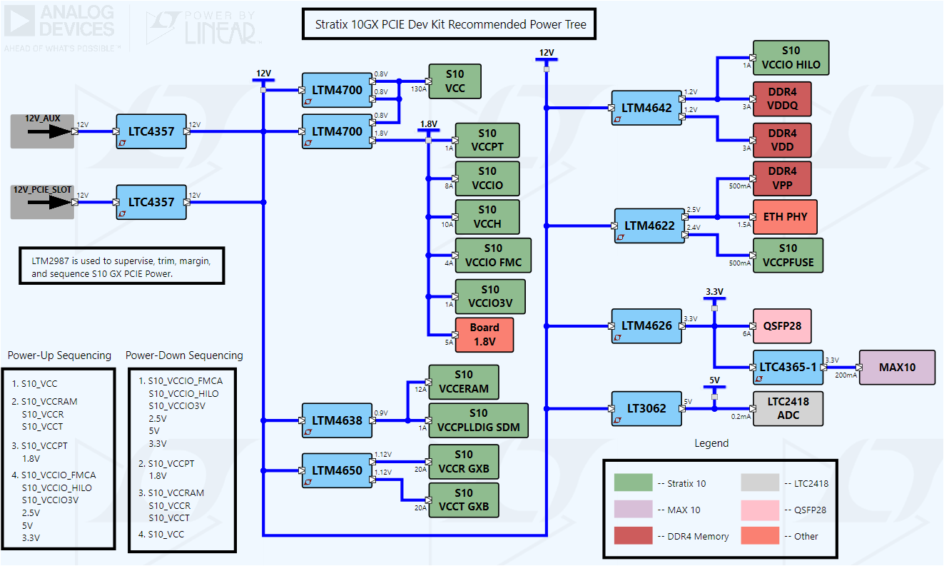
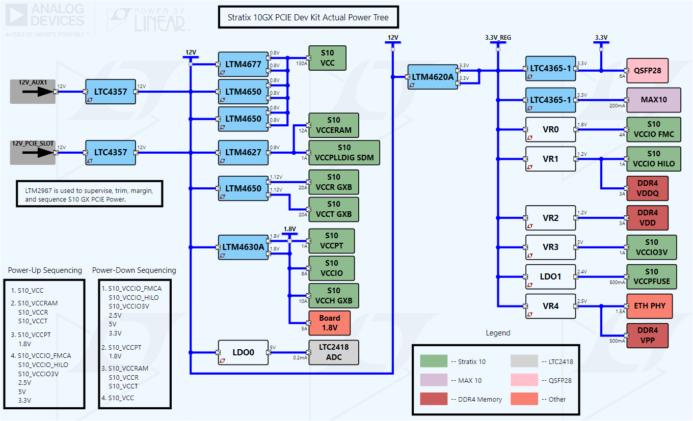
LTM4620Aは、完全なデュアル13Aまたはシングル26A出力のスイッチング・モードDC/DC電源で、LTM4620より出力電圧範囲が広く、高効率です。スイッチング・コントローラ、パワーFET、インダクタ、およびすべての支持部品がパッケージに搭載されています。LTM4620Aは、4.5V~16Vの入力電圧範囲で動作し、出力電圧の範囲がそれぞれ0.6V~5.3Vの2つの出力をサポートしており、出力電圧は1本の外付け抵抗で設定されます。高効率設計により、出力ごとに最大13Aの連続電流を供給します。必要な入力コンデンサおよび出力コンデンサはわずか数個です。
このデバイスは、周波数同期、マルチフェーズ動作、Burst Mode®動作、電源レールのシーケンス制御のための出力電圧トラッキングをサポートしています。また、デバイス温度をモニタするための温度検出ダイオードを内蔵しています。高いスイッチング周波数と電流モード・アーキテクチャにより、安定性を損なうことなく入力および負荷の変動に対するきわめて高速なトランジェント応答が可能です。
フォルト保護機能には、過電圧保護と過電流保護が含まれます。この電源モジュールは、省スペースで熱特性が改善された独自の15mm x 15mm x 4.41mm LGAパッケージと、15mm × 15mm × 5.01mm BGAパッケージで供給されます。LTM4620Aは、SnPb(BGA)またはRoHS準拠の端子仕上げで供給されます。
| Vout Range | Efficiency 12Vin, 1.2Vout | |
| LTM4620 | 0.6V-2.5V | 83% |
| LTM4620A | 0.6V-5.3V | 86% |
アプリケーション
- 通信機器およびネットワーク機器
- 産業用機器
ドキュメント
データシート 2
ユーザ・ガイド 3
技術記事 1
| 製品モデル | ピン/パッケージ図 | 資料 | CADシンボル、フットプリント、および3Dモデル |
|---|---|---|---|
| LTM4620AEV#PBF | 144-Lead LGA (15mm x 15mm x 4.41mm) | ||
| LTM4620AEY#PBF | 144-Lead BGA (15mm x 15mm x 5.01mm) | ||
| LTM4620AIV#PBF | 144-Lead LGA (15mm x 15mm x 4.41mm) | ||
| LTM4620AIY | 144-Lead BGA (15mm x 15mm x 5.01mm) | ||
| LTM4620AIY#PBF | 144-Lead BGA (15mm x 15mm x 5.01mm) | ||
| LTM4620AMPY | 144-Lead BGA (15mm x 15mm x 5.01mm) | ||
| LTM4620AMPY#PBF | 144-Lead BGA (15mm x 15mm x 5.01mm) |
| 製品モデル | 製品ライフサイクル | PCN |
|---|---|---|
|
10 4, 2024 - 24_0225 LTM4620, LTM4620A, LTM4677, LTM4648 and LTM4649 Change of FET |
||
| LTM4620AEV#PBF | 製造中 | |
| LTM4620AEY#PBF | 製造中 | |
| LTM4620AIV#PBF | 製造中 | |
| LTM4620AIY | 製造中 | |
| LTM4620AIY#PBF | 製造中 | |
| LTM4620AMPY | 製造中 | |
| LTM4620AMPY#PBF | 製造中 | |
|
7 28, 2021 - 20_0245 Notification of Wafer Fab Location Change for 0.6µm BICMOS Process Devices from ADI Milpitas (Hillview) to Vanguard Int. (Taiwan) |
||
| LTM4620AEV#PBF | 製造中 | |
| LTM4620AEY#PBF | 製造中 | |
| LTM4620AIV#PBF | 製造中 | |
| LTM4620AIY | 製造中 | |
| LTM4620AIY#PBF | 製造中 | |
| LTM4620AMPY | 製造中 | |
| LTM4620AMPY#PBF | 製造中 | |
|
7 21, 2021 - 21_0159 Ink Mark to Laser Mark Conversion for µModule |
||
| LTM4620AEV#PBF | 製造中 | |
| LTM4620AEY#PBF | 製造中 | |
| LTM4620AIV#PBF | 製造中 | |
| LTM4620AIY | 製造中 | |
| LTM4620AIY#PBF | 製造中 | |
| LTM4620AMPY | 製造中 | |
| LTM4620AMPY#PBF | 製造中 | |
|
2 28, 2020 - 20_0123 Micro-Module, Test Site Transfer from Analog Devices Singapore to Analog Devices Penang, Malaysia |
||
| LTM4620AEV#PBF | 製造中 | |
| LTM4620AEY#PBF | 製造中 | |
| LTM4620AIV#PBF | 製造中 | |
| LTM4620AIY | 製造中 | |
| LTM4620AIY#PBF | 製造中 | |
| LTM4620AMPY | 製造中 | |
| LTM4620AMPY#PBF | 製造中 | |
|
2 5, 2020 - 20_0127 Supplier Material Change for µModule |
||
| LTM4620AEV#PBF | 製造中 | |
| LTM4620AEY#PBF | 製造中 | |
| LTM4620AIV#PBF | 製造中 | |
| LTM4620AIY | 製造中 | |
| LTM4620AIY#PBF | 製造中 | |
| LTM4620AMPY | 製造中 | |
| LTM4620AMPY#PBF | 製造中 | |
|
7 25, 2019 - 19_0167 Notification of Additional Assembly Location, ASE Korea for LTM4620/4620A |
||
| LTM4620AEV#PBF | 製造中 | |
| LTM4620AEY#PBF | 製造中 | |
| LTM4620AIV#PBF | 製造中 | |
| LTM4620AIY | 製造中 | |
| LTM4620AIY#PBF | 製造中 | |
| LTM4620AMPY | 製造中 | |
| LTM4620AMPY#PBF | 製造中 | |
|
11 20, 2023 - 23_0180 New Tray Design for BGA Package |
||
| LTM4620AEY#PBF | 製造中 | |
| LTM4620AIY | 製造中 | |
| LTM4620AIY#PBF | 製造中 | |
| LTM4620AMPY | 製造中 | |
| LTM4620AMPY#PBF | 製造中 | |
これは最新改訂バージョンのデータシートです。
ソフトウェア・リソース
必要なソフトウェア/ドライバが見つかりませんか?
ドライバ/ソフトウェアをリクエストハードウェア・エコシステム
| 製品モデル | 製品ライフサイクル | 詳細 |
|---|---|---|
| µModule 降圧レギュレータ 1 | ||
| LTM4630 | 新規設計に推奨 | デュアル18Aまたはシングル36A DC/DC µModule(パワー・モジュール)レギュレータ |
| PowerPath、理想ダイオード(Ideal Diodes)、負荷スイッチ 1 | ||
| LTC4370 | 新規設計に推奨 | 2電源ダイオードOR電流平衡コントローラ |
| デジタル・パワー・システム・マネージメント(PSM) 1 | ||
| LTC2974 | 新規設計に推奨 | 正確な出力電流測定を特長とする4チャンネルPMBusパワーシステム・マネージャ |
| デジタル・パワー・システム・マネージメント機能を備えた µModule レギュレータ 1 | ||
| LTM4676 | 製造中止 | パワーシステム・マネージメント機能を備えたデュアル13A/シングル26A μModuleレギュレータ |
| 製品モデル | 製品ライフサイクル | 詳細 |
|---|---|---|
| LTM4620 | 製造中 | デュアル13Aまたはシングル26A DC/DC µModuleレギュレータ |
ツールおよびシミュレーション
LTspice 4
- LTM4676/LTM4620A Demo Circuit - High Current, Parallel µModule Buck Regulators with Power System Management (4.5-16V to 1V @100A)
- LTM4620A Demo Circuit - High Efficiency Single 50A Step-Down Regulator (4.5-16V to 1V @ 50A)
- LTM4620A Demo Circuit - High Efficiency Single 26A Step-Down Regulator (4.5-16V to 1V @ 26A)
- LTM4620A Demo Circuit - High Efficiency Dual Buck µModule Regulator (5.5-16V to 3.3 V @ 13A & 5V @ 13A)
下記製品はLTspiceで使用することが出来ます。:
- LTM4620
- LTM4620A
LTpowerCAD 1
次のデバイス用の設計ツールがLTpowerCADでご使用になれます。
- LTM4620
- LTM4620A
LTspice®は、無料で提供される強力で高速な回路シミュレータと回路図入力、波形ビューワに改善を加え、アナログ回路のシミュレーションを容易にするためのモデルを搭載しています。
LTpowerCAD®は、電力段のデバイスの選択、詳細な電力効率の提供、ループのボーデ線図の安定性および負荷過渡応答解析の敏速な表示などを行うと共に、シミュレーション用にLTspiceにエクスポートできる電源設計プログラムです。
評価用キット

LTM4675 + LTM4676A + LTM4677 + LTM4620A Demo Board | PSM μModule Power Stick
資料


LTM4620AEV Demo Board | Dual Buck µModule Regulator, 5.5V ≤ VIN ≤ 16V, VOUT1 = 3.3V @ 13A, VOUT2 = 5V @ 13A
資料


LTM4620AEV Demo Board | 1.5' × 1.2' PCB, Dual Buck µModule Regulator, 5.5V ≤ VIN ≤ 16V, VOUT1 = 3.3V @ 13A, VOUT2 = 1.5V @ 13A
資料
リファレンス・デザイン


使用製品
使用製品
使用製品