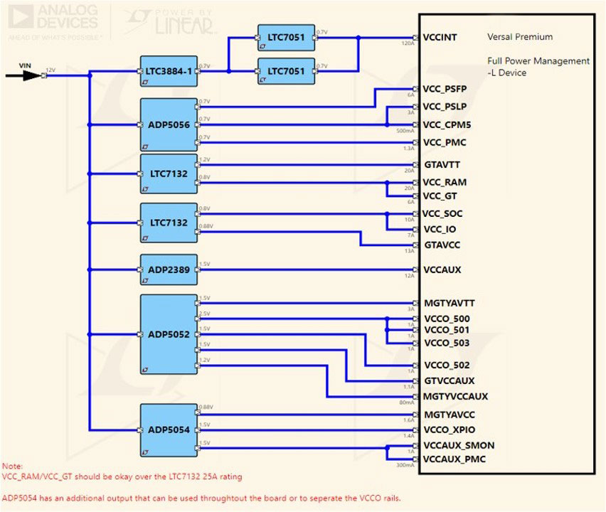
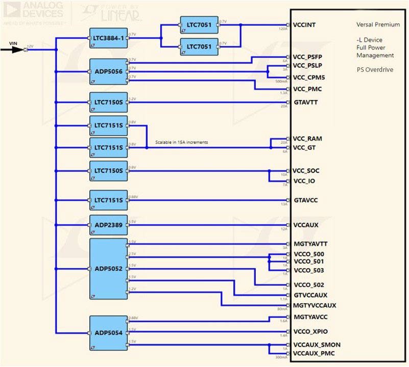
ADP2389

新規設計には非推奨

18 V、12 A、降圧レギュレータ、プログラマブル電流制限回路内蔵

製品モデル
1
1Ku当たりの価格
最低価格:$3.06
利用上の注意

アナログ・デバイセズ社は、提供する情報が正確で信頼できるものであることを期していますが、その情報の利用に関して、あるいはその利用によって生じる第三者の特許やその他の権利の侵害に関して一切の責任を負いません。また、アナログ・デバイセズ社の特許または特許の権利の使用を明示的または暗示的に許諾するものでもありません。仕様は予告なしに変更する場合があります。本紙記載の商標および登録商標は、各社の所有に属します。


本データシートの英語以外の言語への翻訳はユーザの便宜のために提供されるものであり、リビジョンが古い場合があります。最新の内容については、必ず最新の英語版をご参照ください。

なお、日本語版のデータシートは基本的に「Rev.0」(リビジョン0)で作成されています。そのため、英語版が後に改訂され、複数製品のデータシートがひとつに統一された場合、同じ「Rev.0」の日本語版のデータシートが異なる製品のデータシートとして表示されることがあります。たとえば、「ADM3307E」の場合、日本語データシートをクリックすると「ADM3311E」が表示されます。これは、英語版のデータシートが複数の製品で共有できるように1本化され、「ADM3307E/ADM3310E/ADM3311E/ADM3312E/ADM3315E」(Rev.G)と改訂されたからで、決して誤ってリンクが張られているわけではありません。和文化されたデータシートを少しでも有効に活用していただくためにこのような方法をとっておりますので、ご了解ください。

Viewing:

製品の詳細

  • 入力電圧:4.5 V~18 V
  • 連続出力電流:12 A
  • 内蔵MOSFET:ハイサイド17 mΩ/ローサイド4.5 mΩ
  • リファレンス電圧:0.6 V ± 0.5%
  • プログラム可能なスイッチング周波数範囲:200 kHz ~ 2200 kHz
  • 強化された過度応答
  • ±10%精度のプログラマブル電流制限
  • 高精度なイネーブルとパワーグッド
  • 外部補償とソフト・スタート機能
  • プリチャージ出力でのスタートアップ
  • ADIsimPower™ 設計ツールによってサポートされています。

ADP2389

18 V、12 A、降圧レギュレータ、プログラマブル電流制限回路内蔵

ADP2389 Circuit Diagram ADP2389 Pin Configuration
myAnalogに追加

myAnalogの製品セクション(通知受け取り)、既存/新規プロジェクトに製品を追加する。

新規プロジェクトを作成
質問する
サポート

アナログ・デバイセズのサポート・ページはアナログ・デバイセズへのあらゆるご質問にお答えするワンストップ・ポータルです。


ドキュメント

さらに詳しく
myAnalogに追加

myAnalogの製品セクション(通知受け取り)、既存/新規プロジェクトに製品を追加する。

新規プロジェクトを作成

ツールおよびシミュレーション

LTspice 1


下記製品はLTspiceで使用することが出来ます。:

  • ADP2389

ADP2389/ADP2390 Buck Designer Tool

Microsoft Excel download tool from ADIsimPower to generate a power supply design complete with a schematic, bill of materials, and performance specifications.

ツールを開く

SIMPLISモデル 1

LTspice

LTspice®は、無料で提供される強力で高速な回路シミュレータと回路図入力、波形ビューワに改善を加え、アナログ回路のシミュレーションを容易にするためのモデルを搭載しています。


評価用キット

eval board
EVAL-ADP2389

ADP2389 and ADP2390 Evaluation Board

機能と利点

  • Input voltage: 4.5 V to 18 V Continuous output current: 12 A 
  • Integrated MOSFET: 17 mΩ/4.5 mΩ
  • Reference voltage: 0.6 V ±0.5%
  • Programmable switching frequency: 200 kHz to 2.2 MHz 
  • Enhanced transient response
  • Programmable current-limit with ±10% accuracy 
  • Precision enable and power good 
  • External compensation and soft start 
  • PFM mode (ADP2390 only)
  • Start up into a precharged output
  • Supported by ADIsimPower design tool

製品詳細

The ADP2389/ADP2390 evaluation board is a complete, 12 A, 18 V, step-down regulator solution that allows users to evaluate the performance of the ADP2389/ADP2390 with a near ideal printed circuit board (PCB) layout.


The programmable current-limit function allows the inductor to be optimized by output current. The peak current-limit threshold is preset to 21 A to ensure the 12 A output current
capability.


The switching frequency can be programmed between 200 kHz and 2.2 MHz, which provides the possibility for a stackable multiphase power solution.


An enhanced transient response feature improves the load transient performance, which reduces the output capacitance.


The output of the ADP2389/ADP2390 evaluation board is preset to 1.8 V and the switching frequency is set to 500 kHz. Different output voltage settings can be achieved by changing appropriate passive components. The ambient temperature operating range is −40°C to +85°C.


Full details on the ADP2389/ADP2390 regulators are provided in the ADP2389/ADP2390 data sheet, available from Analog Devices, Inc., which should be consulted in conjunction with this user guide.

EVAL-ADP2389
ADP2389 and ADP2390 Evaluation Board
ADP2389-EVALZ_ADP2390-EVALZ

リファレンス・デザイン

Full Power Management (-L Devices)​
Versal Premium Circuits from the Lab®

Non-Hardware Verified Design

機能と利点

  • Xilinx Versal Premium series solves a broad range of industry-specific problems with performance and flexibility. Core use cases include storage acceleration, data center network acceleration, 5G xHaul and Passive optical networks.

  • Analog Devices, Inc. supports power delivery solutions for the Versal Premium Platform. Monolithic solutions are used on the Versal Premium Platform to power Xilinx FPGA and/or SoC rails as well as other system rails. These regulators are highly integrated discrete solutions optimized for cost, efficiency and footprint.

  • ADI provides supporting documentation including power schematics, layout, LTpowerPlanner® and applicable LTpowerPlay® configuration files to enable you to validate the power solution for your application seamlessly.

  • For a complete list power designs and use cases, please contact your local FAE.

  • Key Power for full management devices are used as follows:

    • LTC3884-1
    • LTC7051
    • ADP5056
    • LTC7132
    • ADP2389
    • ADP5052
    • ADP5054
    • LTC7150S
    • LTC7151S
Versal Premium
Non-Hardware Verified Design
Full Power Management (-L Devices)​
Full Power Management (-L Devices) PS Overdrive

最新のディスカッション

最近表示した製品