ADM7154
ADM7154
新規設計に推奨RFリニア電圧レギュレータ、600mA、超低ノイズ、高PSRR
- 製品モデル
- 12
- 1Ku当たりの価格
- 最低価格:$2.75
Viewing:
製品の詳細
- 入力電圧範囲:2.3V~5.5V
- 最大負荷電流:600mA
- 低ノイズ
- 総合積分ノイズ:0.9µV rms(100Hz~100kHz)
- 総合積分ノイズ:1.6µV rms(10Hz~100kHz)
- ノイズ・スペクトル密度: 1.5nV/√Hz(10kHz~1MHz)
- PSRR:90dB(200Hz~200kHz);58dB@1MHz、 VOUT=3.3V、VIN=3.8V
- ドロップアウト電圧:120mV(typ)@VOUT=3.3V、IOUT=600mA
- 初期精度:±0.5%
- ライン、負荷、温度についての精度(−40°C ~ +85°C):-2.0%(min)、+1.5%(max)
- 静止時電流、IGND=4mA(無負荷)
- 低シャットダウン電流:0.2 μA
- 10 μFのセラミック出力コンデンサで安定
- 調整可能/固定出力電圧オプション:1.2 V、1.8 V、2.5 V、2.8 V、3.0 V、3.3 V(1.2~3.3 Vの中の16の標準電圧を用意)
- 8ピンLFCSPと8ピンSOICパッケージ
- 高精度イネーブル入力
- ADIsimPowerツール対応
ADM7154は2.3V~5.5Vで動作し、最大600mAの出力電流を供給するリニア・レギュレータです。先進的な独自のアーキテクチャを採用する事により、高い電源電圧除去、超低ノイズ特性を実現し、小さな10μFのセラミック出力コンデンサだけで、優れたラインおよび負荷過度応答が得られます。
ADM7154には16種類の標準的な出力電圧が用意されています。次の電圧は常備品です。1.2V、1.8V、2.5V、3.0V、2.8V、3.0V、3.3V。次の電圧は特注によってご用意できます:1.3V、1.5 V、1.6V、2.0V、2.2V、2.6V、2.7V、2.9V、3.1V、3.2V。
レギュレータADM7154の出力ノイズは固定出力オプションの場合0.9μV rms typ(100Hz~100kHz)で、ノイズ・スペクトル密度は1.5nV/√Hz(10kHz~1MHz)です。
ADM7154は、8ピンの3mm×3mm LFCSPと8ピンSOICパッケージを採用し、非常にコンパクトなソリューソンを実現できるだけではなく、小型、薄型フットプリントにおいて最大600mAの出力電流が要求されるアプリケーションに対して優れた熱性能を提供します。
アプリケーション
- ノイズに敏感なアプリケーションのレギュレーション:PLL、VCO、VCO内蔵のPLL
- 通信関連およびインフラストラクチャ
- バックホール、マイクロウェーブ・リンク
ドキュメント
データシート 2
ユーザ・ガイド 2
アプリケーション・ノート 1
ビデオ 4


ソリューション・カタログ 2
Analog Dialogue 1
| 製品モデル | ピン/パッケージ図 | 資料 | CADシンボル、フットプリント、および3Dモデル |
|---|---|---|---|
| ADM7154ACPZ-1.2-R7 | 8-Lead LFCSP (3mm x 3mm w/ EP) | ||
| ADM7154ACPZ-1.8-R7 | 8-Lead LFCSP (3mm x 3mm w/ EP) | ||
| ADM7154ACPZ-2.5-R7 | 8-Lead LFCSP (3mm x 3mm w/ EP) | ||
| ADM7154ACPZ-2.8-R7 | 8-Lead LFCSP (3mm x 3mm w/ EP) | ||
| ADM7154ACPZ-3.0-R7 | 8-Lead LFCSP (3mm x 3mm w/ EP) | ||
| ADM7154ACPZ-3.3-R7 | 8-Lead LFCSP (3mm x 3mm w/ EP) | ||
| ADM7154ARDZ-1.2-R7 | 8-Lead SOIC w/ EP | ||
| ADM7154ARDZ-1.8-R7 | 8-Lead SOIC w/ EP | ||
| ADM7154ARDZ-2.5-R7 | 8-Lead SOIC w/ EP | ||
| ADM7154ARDZ-2.8-R7 | 8-Lead SOIC w/ EP | ||
| ADM7154ARDZ-3.0-R7 | 8-Lead SOIC w/ EP | ||
| ADM7154ARDZ-3.3-R7 | 8-Lead SOIC w/ EP |
これは最新改訂バージョンのデータシートです。
ソフトウェア・リソース
必要なソフトウェア/ドライバが見つかりませんか?
ドライバ/ソフトウェアをリクエストハードウェア・エコシステム
| 製品モデル | 製品ライフサイクル | 詳細 |
|---|---|---|
| ADM7155 | 新規設計に推奨 |
RFリニア電圧レギュレータ、600mA、超低ノイズ、高PSRR |
ツールおよびシミュレーション
LTspice
下記製品はLTspiceで使用することが出来ます。:
- ADM7154-1.2
- ADM7154-1.8
- ADM7154-2.5
- ADM7154-3.0
- ADM7154-3.3
LTspice®は、無料で提供される強力で高速な回路シミュレータと回路図入力、波形ビューワに改善を加え、アナログ回路のシミュレーションを容易にするためのモデルを搭載しています。
評価用キット


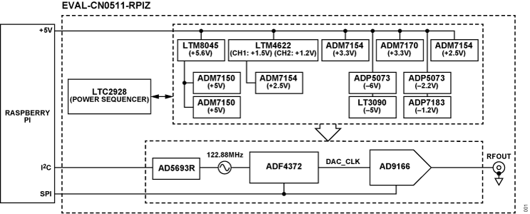
Direct RF to Baseband Transmit Radio
資料


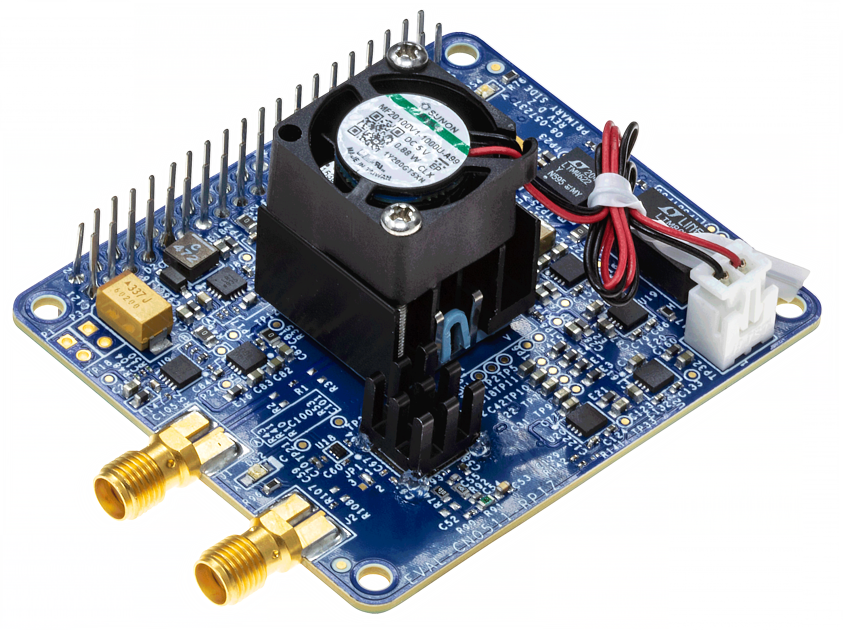
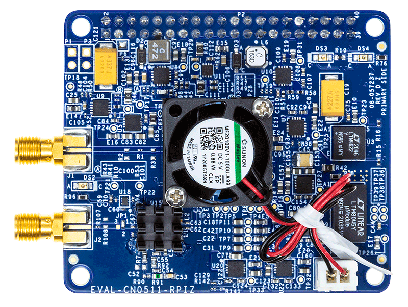
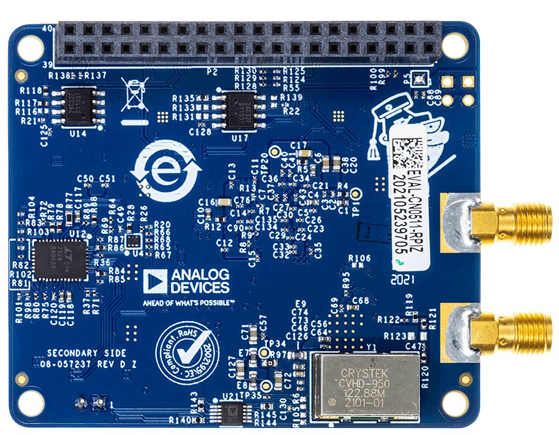
ADM7154 Evaluation Board
資料


TX/RXチャンネル、1~100MHzから最大400MHzへの周波数変換
資料
ソフトウェア


HMCAD1511 Evaluation Board
資料
ソフトウェア
HMCAD1520 Evaluation Board
資料
ソフトウェア


ADA4961 & AD9680 Analog Signal Chain Evaluation and AD9528 Converter Synchronization
資料
ソフトウェア


マルチチャンネル・システム・クロッキング・デバイス
資料


10Gbイーサネット・アダプタへのFPGAベースの8x GMSL
資料
ソフトウェア
リファレンス・デザイン
出力電力が+/−0.5dBに補正されたDC~5.5GHzの信号発生器 ※Rev.0 を翻訳したものです。最新版は英語資料をご覧ください。