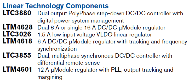
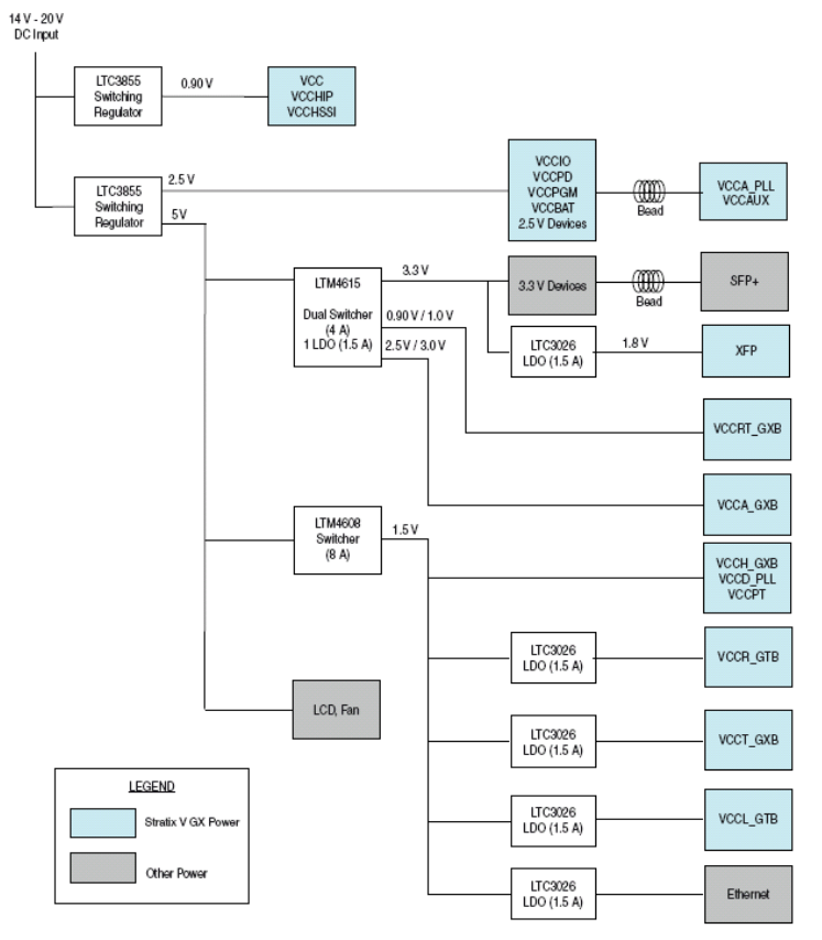
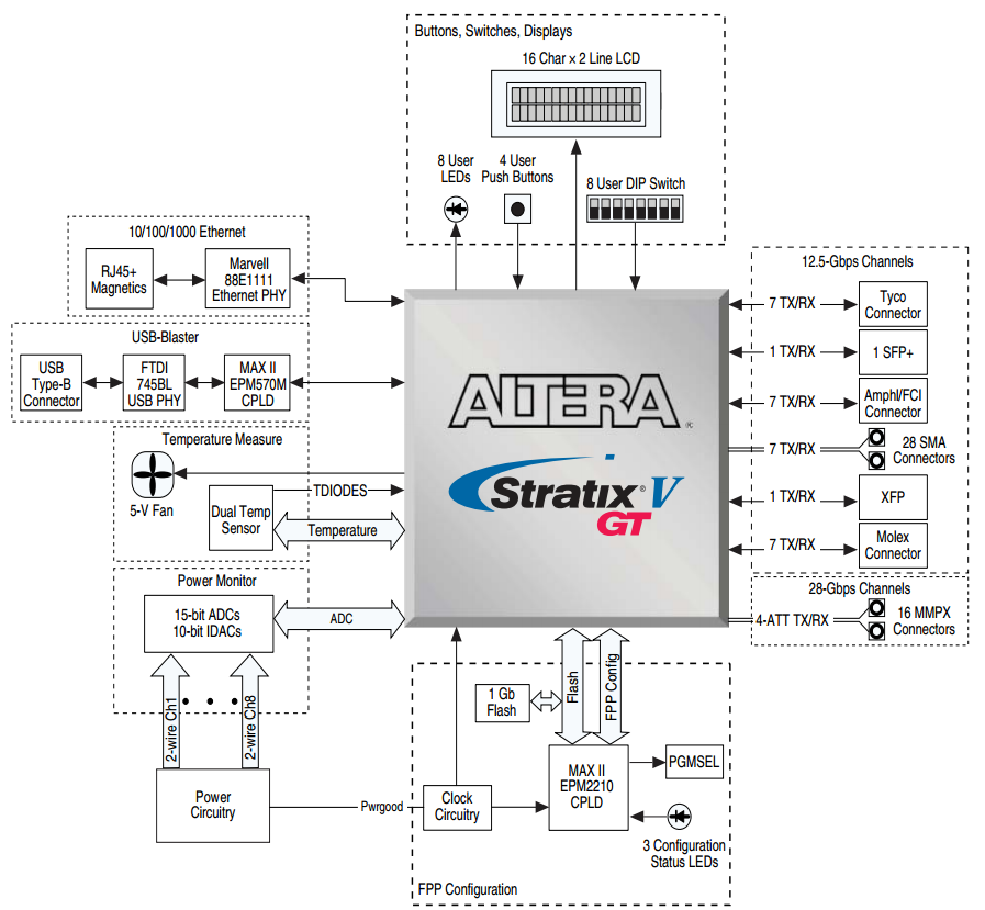
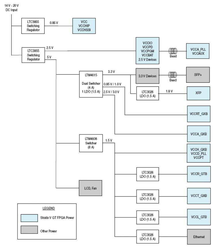
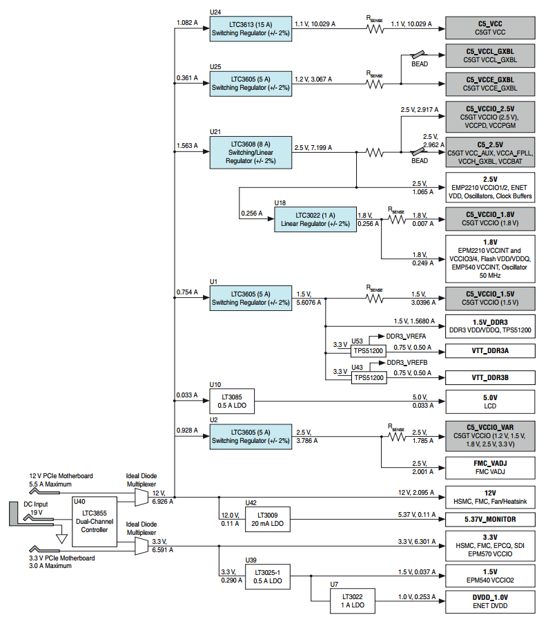
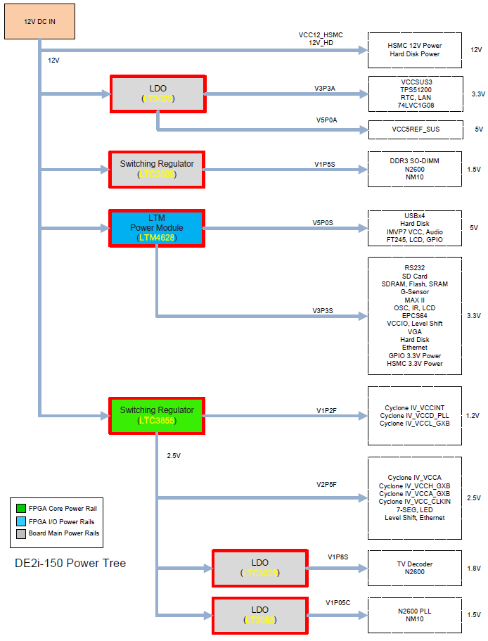
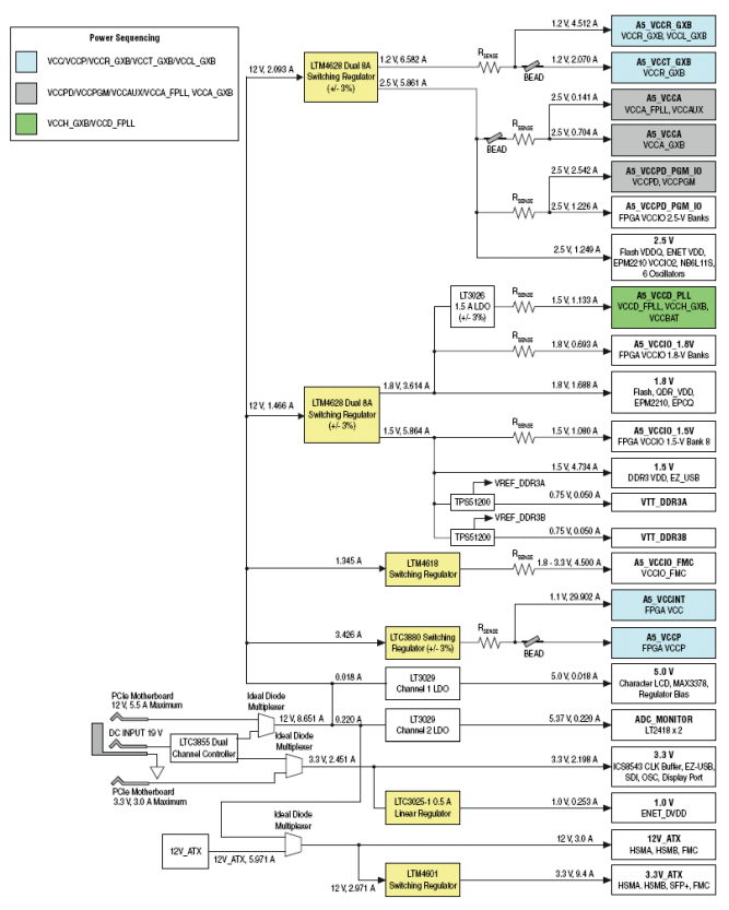
LTC3855
量产采用差分远端采样的双通道、多相、同步 DC/DC 控制器
- 产品模型
- 8
产品详情
- 双通道、180° 定相控制器降低了所需的输入电容和电源感应噪声
- 高效率:达 95%
- RSENSE 或 DCR 电流检测
- 可编程 DCR 温度补偿
- ±0.75%、0.6V 输出电压准确度
- 可锁相固定频率:250kHz 至 770kHz
- 真正的远端采样差分放大器
- 双路 N 沟道 MOSFET 同步驱动
- 宽 VIN 范围:4.5V 至 38V
- VOUT 范围:0.6V 至 12.5V (未采用差分放大器)
- VOUT 范围:0.6V 至 3.3V (采用差分放大器)
- 用于多达 12 相运作的时钟输入和输出
- 可调软起动或 VOUT 跟踪
- 折返输出电流限制
- 输出过压保护
- 40 引脚 (6mm x 6mm) QFN 封装和 38 引脚 FE 封装
LTC®3855 是一款双通道、多相 (PolyPhase®)、电流模式、同步降压型开关稳压控制器,用于驱动全 N 沟道功率 MOSFET 级。该器件内置了一个高速差分远端采样放大器。最大电流检测电压可针对 30mV、50mV 或 70mV 进行设置,因而允许使用电感器 DCR 或一个分立的检测电阻器作为检测元件。
LTC3855 具有一个精准的 0.6V 基准,并能够产生高达 12.5V 的输出电压。4.5V 至 38V 的宽输入电源范围囊括了大多数中间总线电压和电池化学组成。通过使两个控制器输出级异相运作,较大限度地降低了功率损失和电源噪声。该器件可支持突发模式 (Burst Mode®) 操作、连续或脉冲跳跃模式。
LTC3855 可以针对多达 12 相操作进行配置,具有 DCR 温度补偿、两个电源良好信号和两个电流限值设定引脚。LTC3855 采用扁平的 40 引脚 6mm x 6mm QFN 封装和 38 引脚裸露衬垫 FE 封装。
应用
- 计算机系统
- 电信系统
- 工业和医疗仪器 DC 功率分配系统
参考资料
数据手册 1
可靠性数据 1
用户手册 3
应用笔记 2
设计笔记 1
技术文章 3
ADI 始终高度重视提供符合最高质量和可靠性水平的产品。我们通过将质量和可靠性检查纳入产品和工艺设计的各个范围以及制造过程来实现这一目标。出货产品的“零缺陷”始终是我们的目标。查看我们的质量和可靠性计划和认证以了解更多信息。
| 产品型号 | 引脚/封装图-中文版 | 文档 | CAD 符号,脚注和 3D模型 |
|---|---|---|---|
| LTC3855EFE#PBF | 38-Lead TSSOP w/ EP | ||
| LTC3855EFE#TRPBF | 38-Lead TSSOP w/ EP | ||
| LTC3855EUJ#PBF | 40-Lead QFN (6mm x 6mm x 0.75mm w/ EP) | ||
| LTC3855EUJ#TRPBF | 40-Lead QFN (6mm x 6mm x 0.75mm w/ EP) | ||
| LTC3855IFE#PBF | 38-Lead TSSOP w/ EP | ||
| LTC3855IFE#TRPBF | 38-Lead TSSOP w/ EP | ||
| LTC3855IUJ#PBF | 40-Lead QFN (6mm x 6mm x 0.75mm w/ EP) | ||
| LTC3855IUJ#TRPBF | 40-Lead QFN (6mm x 6mm x 0.75mm w/ EP) |
| 产品型号 | 产品生命周期 | PCN |
|---|---|---|
|
2月 14, 2025 - 25_0017 Bond Wire Change from Gold to Copper |
||
| LTC3855EFE#PBF | 量产 | |
| LTC3855EFE#TRPBF | 量产 | |
| LTC3855EUJ#PBF | 量产 | |
| LTC3855EUJ#TRPBF | 量产 | |
| LTC3855IFE#PBF | 量产 | |
| LTC3855IFE#TRPBF | 量产 | |
|
4月 6, 2022 - 22_0068 Laser Top Mark for ETSSOP and TSSOP Packages Assembled in ADPG [PNG] and UTL |
||
| LTC3855EFE#PBF | 量产 | |
| LTC3855EFE#TRPBF | 量产 | |
| LTC3855IFE#PBF | 量产 | |
| LTC3855IFE#TRPBF | 量产 | |
|
11月 8, 2021 - 20_0245 Notification of Wafer Fab Location Change for 0.6µm BICMOS Process Devices from ADI Milpitas (Hillview) to Vanguard Int. (Taiwan) |
||
| LTC3855EFE#PBF | 量产 | |
| LTC3855EFE#TRPBF | 量产 | |
| LTC3855EUJ#PBF | 量产 | |
| LTC3855EUJ#TRPBF | 量产 | |
| LTC3855IFE#PBF | 量产 | |
| LTC3855IFE#TRPBF | 量产 | |
| LTC3855IUJ#PBF | 量产 | |
| LTC3855IUJ#TRPBF | 量产 | |
这是最新版本的数据手册
软件资源
找不到您所需的软件或驱动?
申请驱动/软件硬件生态系统
工具及仿真模型
LTspice 1
LTspice中提供以下器件型号:
- LTC3855
LTpowerCAD 6
- LTC3855 Project - Dual, 2-Phase Synchronous Step-Down Controller with Rsense Current Sensing (4.5-26V to 2.5V @ 15A & 1.8V @ 15A)
- LTC3855 Project - Dual, 2-Phase Synchronous Step-Down Controller with Rsense Current Sensing (4.5-14V to 1.8V @ 17A & 1.2V @ 17A)
- LTC3855 Project - Dual, 2-Phase Synchronous Step-Down Controller with Rsense Current Sensing (13-36V to 12V @ 6A & 5V @ 10A)
- LTC3855 Project - Dual, 2-Phase Synchronous Step-Down Controller with Inductor DCR Current Sensing (4.5-26V to 2.5V @ 15A & 1.8V @ 15A)
- LTC3855 Project - Dual, 2-Phase Synchronous Step-Down Controller with Inductor DCR Current Sensing (13-36V to 12V @ 6A & 5V @ 10A)
- LTC3855 Project - Dual, 2-Phase Synchronous Step-Down Controller with Inductor DCR Current Sensing (4.5-14V to 1.8V @ 17A & 1.2V @ 17A)
LTpowerCAD中提供以下器件的设计工具:
- LTC3855
LTspice®是一款强大高效的免费仿真软件、原理图采集和波形观测器,为改善模拟电路的仿真提供增强功能和模型。
LTpowerCAD®是一种电源设计程序,它选择功率级元件,提供详细效率信息,显示快速环路波特图稳定性和负载瞬态分析,并可导出至LTspice进行仿真。
评估套件
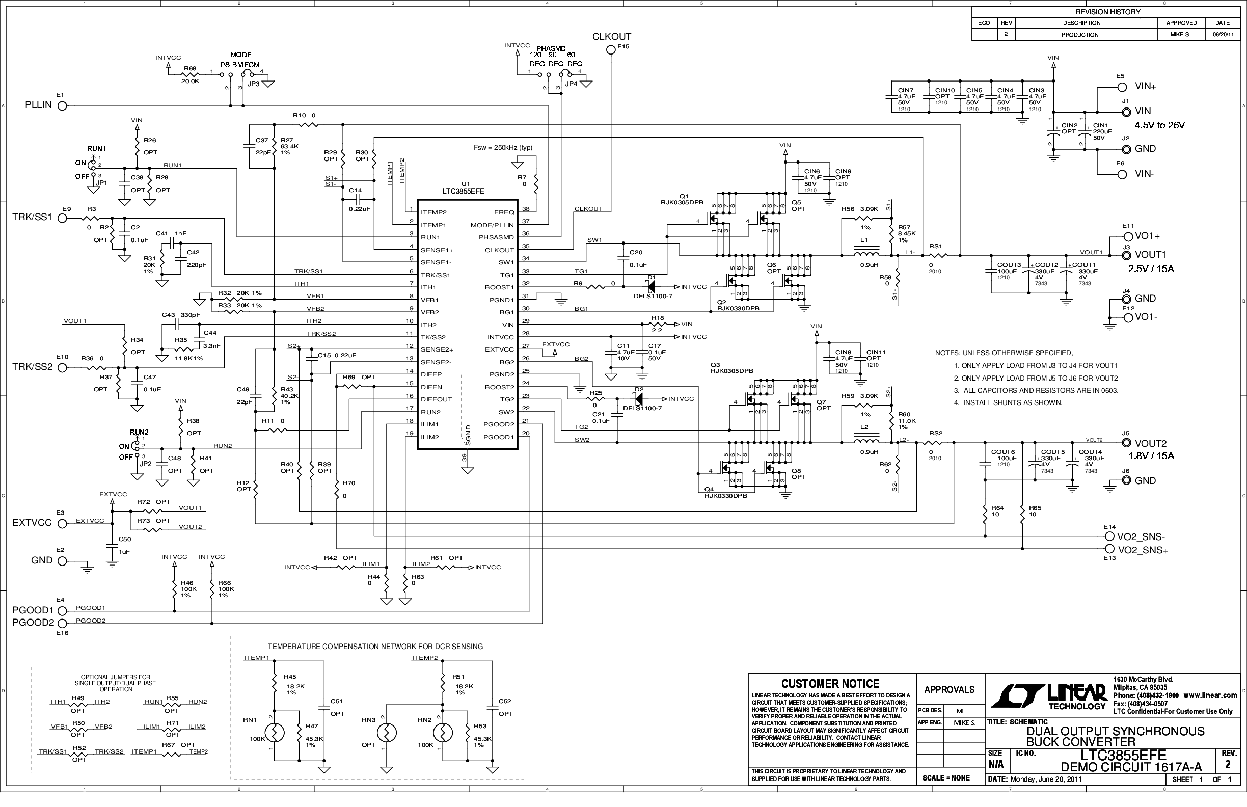
LTC3855EFE Demo Board | Dual Output VIN = 4.5V to 26V, VOUT1 = 2.5V @ 15A, VOUT2 = 1.8V @ 15A
资料
LTC3855EFE Demo Board | Dual Output VIN = 13V to 36V, VOUT1 = 12V @ 6A, VOUT2 = 5V @ 10A
资料
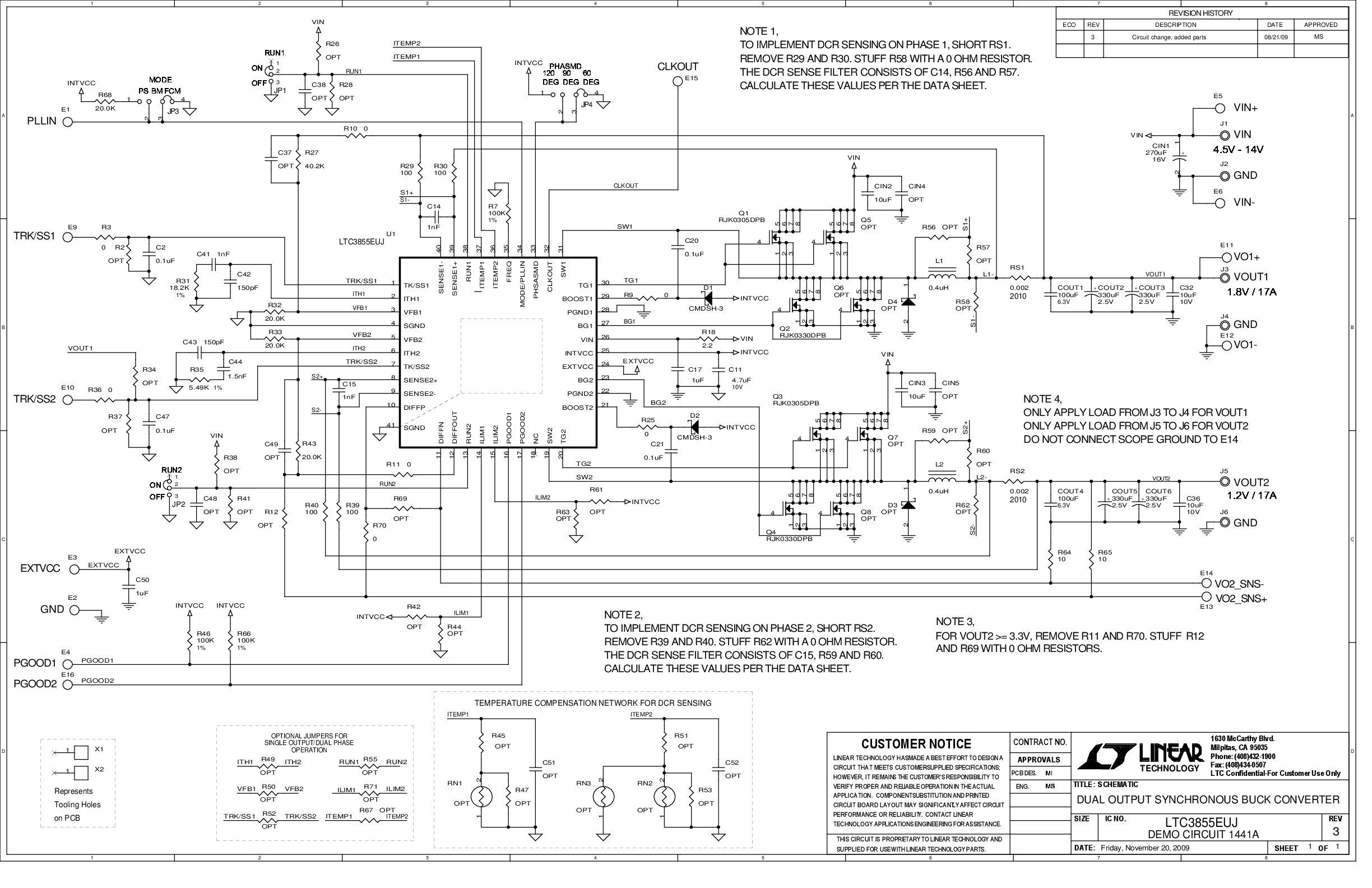
LTC3855EUJ演示板 | 双路输出, VIN = 4.5V 至 14V, VOUT1 = 1.8V (17A), VOUT2 = 1.2V (17A)
资料
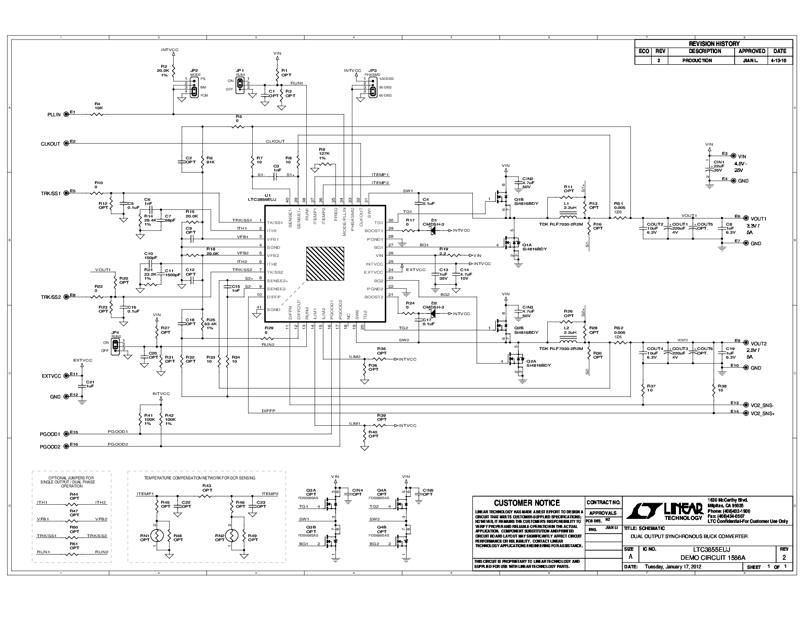
LTC3855EUJ Demo Board | Dual Output, VIN = 4.5V to 25V, VOUT1 = 3.3V @ 5A, VOUT2 = 2.5V @ 5A
资料
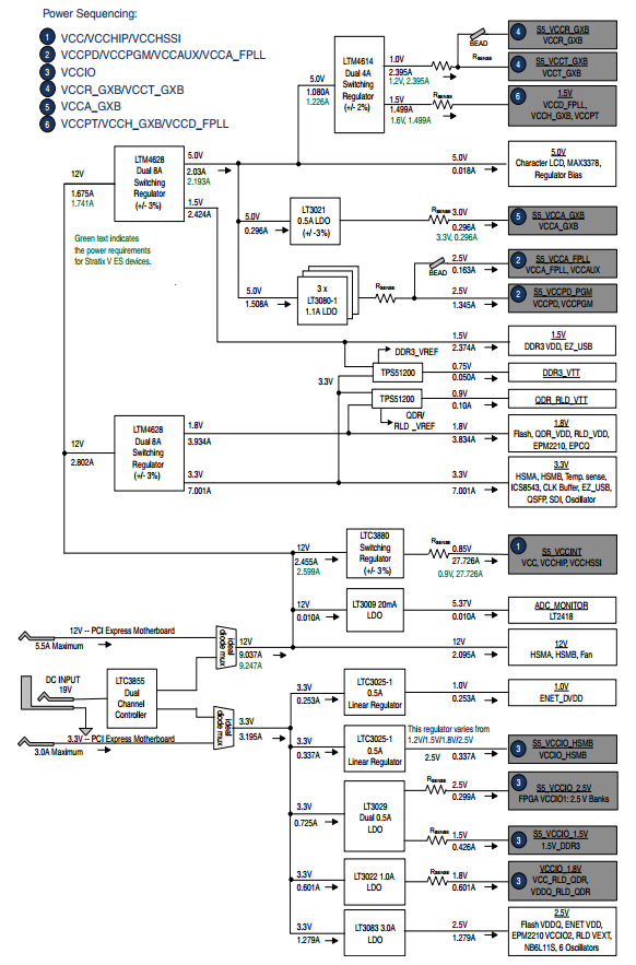
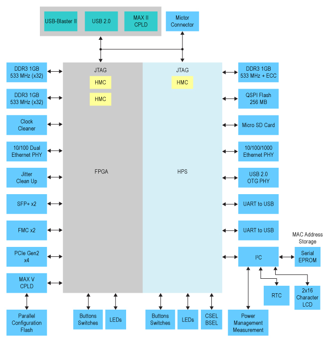
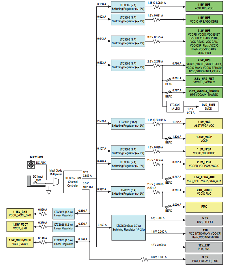
参考电路
使用部分
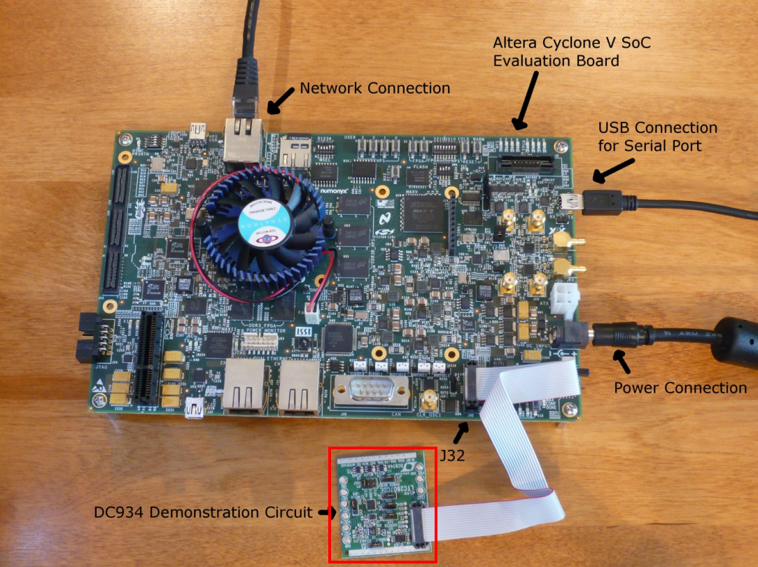
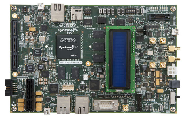
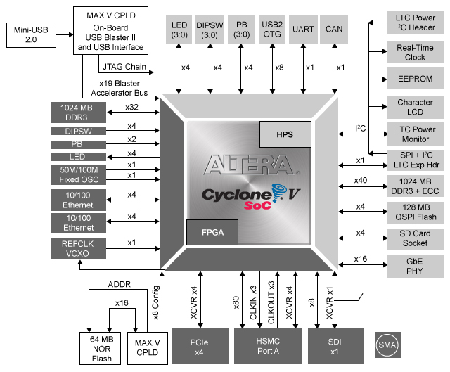
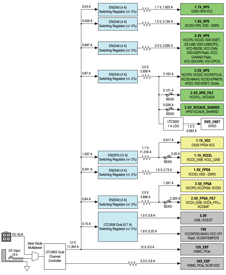
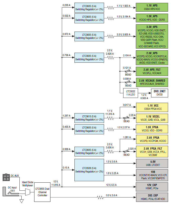

使用部分
使用部分

使用部分


使用部分
最新评论
需要发起讨论吗? 没有关于 LTC3855的相关讨论?是否需要发起讨论?
在EngineerZone®上发起讨论