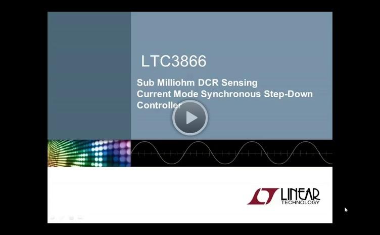
LTC3866
推荐用于新设计用于 mΩ 以下 DCR 检测的电流模式同步控制器
- 产品模型
- 8
产品详情
- mΩ 以下 DCR 电流检测
- 高效率:达 95%
- 可选的电流检测限值
- 可编程 DCR 温度补偿
- 硅片过温热停机
- ±0.5% 0.6V 输出电压准确度
- 可编程固定频率:250kHz 至 770kHz
- 高速差分远端采样放大器
- 宽输入电压范围:4.5V 至 38V
- 输出电压范围:0.6V 至 3.5V (采用差分放大器)
- 可调软起动或输出电压跟踪
- 折返输出电流限制
- 短路软恢复
- 输出过压保护
- 24 引线 (4mm x 4mm) QFN 封装和 24 引线 FE 封装
LTC®3866 是一款单相电流模式同步降压型开关稳压控制器,用于驱动全 N 沟道功率 MOSFET 开关。该器件采用了一种独特的架构,此架构可改善电流检测信号的信噪比,从而允许使用非常低 DC 电阻的功率电感器,以较大限度地提升高电流应用中的效率。该特性还降低了低 DCR 应用中常见的开关抖动。另外,LTC3866 还包括一个高速远端采样差分放大器、一个可选择为 10mV、15mV、20mV、25mV 或 30mV 的可编程电流检测限值以及 DCR 温度补偿功能电路,旨在精确限制整个温度范围内的最大输出电流。
LTC3866 还具有一个 0.6V 的高精度基准和一个 ±0.5% 的保证限值,可提供一个 0.6V 至 3.5V 的准确输出电压。一个 4.5V 至 38V 的输入电压范围允许它支持众多的总线电压与各种类型的电池。
LTC3866 可提供扁平 24 引线 4mm x 4mm QFN 封装和 24 引线裸露衬垫 FE 封装。
应用
- 计算机系统
- 电信系统
- 工业和医疗仪器
- DC 功率分配系统
参考资料
数据手册 1
可靠性数据 1
用户手册 1
应用笔记 1
技术文章 3
视频 2
解决方案设计及宣传手册 1
新闻 1
ADI 始终高度重视提供符合最高质量和可靠性水平的产品。我们通过将质量和可靠性检查纳入产品和工艺设计的各个范围以及制造过程来实现这一目标。出货产品的“零缺陷”始终是我们的目标。查看我们的质量和可靠性计划和认证以了解更多信息。
| 产品型号 | 引脚/封装图-中文版 | 文档 | CAD 符号,脚注和 3D模型 |
|---|---|---|---|
| LTC3866EFE#PBF | 24-Lead TSSOP w/ EP | ||
| LTC3866EFE#TRPBF | 24-Lead TSSOP w/ EP | ||
| LTC3866EUF#PBF | 24-Lead QFN (4mm x 4mm x 0.75mm w/ EP) | ||
| LTC3866EUF#TRPBF | 24-Lead QFN (4mm x 4mm x 0.75mm w/ EP) | ||
| LTC3866IFE#PBF | 24-Lead TSSOP w/ EP | ||
| LTC3866IFE#TRPBF | 24-Lead TSSOP w/ EP | ||
| LTC3866IUF#PBF | 24-Lead QFN (4mm x 4mm x 0.75mm w/ EP) | ||
| LTC3866IUF#TRPBF | 24-Lead QFN (4mm x 4mm x 0.75mm w/ EP) |
| 产品型号 | 产品生命周期 | PCN |
|---|---|---|
|
2月 14, 2025 - 25_0016 Bond Wire Change from Gold to Copper Wire (Notification Only) |
||
| LTC3866EFE#PBF | 量产 | |
| LTC3866EFE#TRPBF | 量产 | |
| LTC3866EUF#PBF | 量产 | |
| LTC3866EUF#TRPBF | 量产 | |
| LTC3866IFE#PBF | 量产 | |
| LTC3866IFE#TRPBF | 量产 | |
|
4月 6, 2022 - 22_0068 Laser Top Mark for ETSSOP and TSSOP Packages Assembled in ADPG [PNG] and UTL |
||
| LTC3866EFE#PBF | 量产 | |
| LTC3866EFE#TRPBF | 量产 | |
| LTC3866IFE#PBF | 量产 | |
| LTC3866IFE#TRPBF | 量产 | |
|
1月 20, 2022 - 21_0269 Addition of Alternate Assembly Site ASE Taiwan for Select LFCSP Products |
||
| LTC3866EUF#PBF | 量产 | |
| LTC3866EUF#TRPBF | 量产 | |
| LTC3866IUF#PBF | 量产 | |
| LTC3866IUF#TRPBF | 量产 | |
|
4月 9, 2025 - 25_0016 Bond Wire Change from Gold to Copper Wire (Notification Only) |
||
| LTC3866IUF#PBF | 量产 | |
| LTC3866IUF#TRPBF | 量产 | |
这是最新版本的数据手册
软件资源
找不到您所需的软件或驱动?
申请驱动/软件硬件生态系统
工具及仿真模型
LTspice 2
- LTC3866 Demo Circuit - High Efficiency, Synchronous Step-Down Converter with Sub mΩ Inductor DCR Sensing (4.5-20V to 1.5V @ 30A)
- LTC3866 Demo Circuit - High Efficiency 12V Input, 5V/25A Step-Down Converter (12V to 5V @ 25A)
LTspice中提供以下器件型号:
- LTC3866
LTpowerCAD 1
LTpowerCAD中提供以下器件的设计工具:
- LTC3866
LTspice®是一款强大高效的免费仿真软件、原理图采集和波形观测器,为改善模拟电路的仿真提供增强功能和模型。
LTpowerCAD®是一种电源设计程序,它选择功率级元件,提供详细效率信息,显示快速环路波特图稳定性和负载瞬态分析,并可导出至LTspice进行仿真。
评估套件
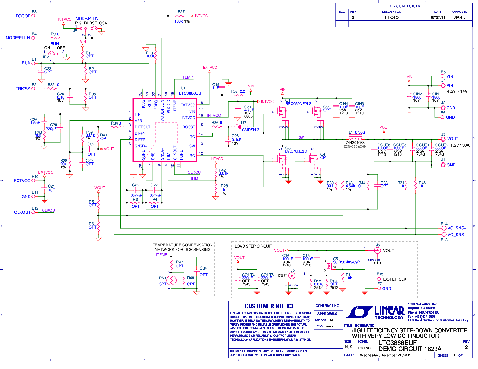
LTC3866EUF Demo Board VIN = 4.5V to 14V, VOUT = 1.5V @ 30A
资料
参考电路
最新评论
需要发起讨论吗? 没有关于 LTC3866的相关讨论?是否需要发起讨论?
在EngineerZone®上发起讨论