CN0255


Overview
Design Resources
Design & Integration File
- Schematic
- Bill of Materials
- Gerber Files
- PADS Files
- Assembly Drawing
Evaluation Hardware
Part Numbers with "Z" indicate RoHS Compliance. Boards checked are needed to evaluate this circuit.
- EVAL-CN0255-SDPZ ($92.98) A Complete Single-Supply, 16-Bit, 100 kSPS PulSAR ADC System Dissipates 8 mW
- EVAL-SDP-CB1Z ($116.52) Eval Control Board
Device Drivers
Software such as C code and/or FPGA code, used to communicate with component's digital interface.
Features & Benefits
- 16-bit, 100KSPS Data Acquisiton
- Single Supply
- 8mW Total Power
Product Categories
Markets and Technologies
Parts Used
Documentation & Resources
-
MT-101: Decoupling Techniques2/14/2015PDF954 kB
-
MT-021: ADC Architectures II: Successive Approximation ADCs2/14/2015PDF3799 kB
-
MT-031: Grounding Data Converters and Solving the Mystery of "AGND" and "DGND"3/20/2009PDF144 kB
-
CN-0255: A Complete Single-Supply, 16-Bit, 100 kSPS PulSAR ADC System Dissipates 8 mW12/30/2013PDF325 kB
Circuit Function & Benefits
In most systems, there are trade-offs between performance and low power. The focus of this circuit design is to explore a few of these trade-offs and still achieve low power (8 mW typical) and high performance in a 16-bit, 100 kSPS data acquisition system.
This circuit uses the AD7988-1, a low power (350 μA) PulSAR® analog-to-digital converter (ADC), driven directly from the ADA4841-1 high performance, low voltage, low power op amp. This amplifier was chosen for its excellent dynamic performance and its ability to operate with a single-supply voltage and to provide a rail-to-rail output. In addition, the input common-mode voltage range includes the negative rail.
The AD7988-1 ADC requires an external voltage reference between 2.4 V and 5.1 V. In this application, the voltage reference chosen was the ADR4525 precision 2.5 V reference.


Circuit Description
The heart of this circuit is the AD7988-1, a 16-bit, 100 kSPS successive approximation, ADC that operates from a single VDD power supply. It contains a low power, high speed, 16-bit sampling ADC and a versatile serial port interface (SPI). On the CNV rising edge, it samples an analog input, IN+, between 0 V to REF with respect to the ground sense pin, IN−. The reference voltage, REF, is applied externally and can be set independent of the supply voltage, VDD.
For the experiments carried out for this circuit note, the AD7988-1 evaluation board was interfaced to the System Demonstration Platform (SDP), EVAL-SDP-CB1Z, where the ADC SPI-compatible serial interface was connected to the DSP SPORT interface. The ADCs SPI interface features the ability to daisy-chain several ADCs on a single 3-wire bus. It is compatible with 1.8 V, 2.5 V, 3 V, or 5 V logic, using the separate VIO supply pin.
The AD7988-1 is housed in a 10-lead MSOP or a 10-lead QFN (LFCSP). This board uses the MSOP package for convenience.
The ADC input is buffered and driven from the ADA4841-1, a unity-gain stable, low noise and low distortion, rail-to-rail output amplifier that operates with a quiescent current of 1.1 mA typically. This amplifier offers a low wideband voltage noise of 2.1 nV/√Hz and 1.4 pA/√Hz current noise, along with excellent spurious-free dynamic range (SFDR) of −105 dBc at 100 kHz. To maintain a low noise environment at lower frequencies, the amplifiers have low 1/f noise of 7 nV/√Hz and 13 pA/√Hz at 10 Hz.
A key feature of the ADA4841-1, making it ideally suited to single-supply applications, is that in this application it can operate from a single rail, with the negative rail tied to ground. The amplifier output can swing to within 50 mV of the ground level, which is acceptable for this application. Note that the input common-mode voltage range extends from the negative supply rail to within 1 V of the positive rail. This necessitates 1 V headroom to accommodate the signal range of interest (0 V to 2.5 V); therefore, in this circuit, a 4 V rail was used. The ADA4841-1 is available in a 6-lead SOT-23 or an 8-lead SOIC.
The 2.5 V voltage reference used in this application is the ADR4525 from the ADR45xx series of references, providing high precision, low power, low noise, and featuring ±0.01% initial accuracy, excellent temperature stability, and low output noise. System performance is improved by the ADR4525 low thermally induced output voltage hysteresis and low long-term output voltage drift. A maximum operating current of 700 μA and a low dropout voltage of 500 mV maximum make the device optimum for use in portable equipment.
Each of the three products used in the circuit are rated for operation over the full industrial temperature range, −40°C to +125°C.
Performance Expectations
Because power is key in this application, an analysis of each of the component's contribution is necessary to ensure appropriate selection among the many available products. The first step was reviewing the different supply currents for the three devices selected.
The typical calculated and measured supply currents are shown in Table 1 for each of the contributing components. The VIO supply from the digital interface of the ADC is not included here because it is negligible. The measured currents compare favorably with the calculated values; the small discrepancy can be attributed to the passive components and slight variations in supply currents from that of the typical data sheet specifications.
| Load | Description | Calculated |
Measured | ||||
| Supply Current | Supply Voltage | Power | Supply Current | Supply Voltage | Power | ||
| ADC | AD7988-1 | 150 µA | 2.5 V | 375 µW | 148 µA |
2.5 V | 370 µW |
| Driver | ADA4841-1 | 1.1 mA | 4 V | 4.4 mW | 1.95 mA | 4 V | 7.8 mW |
| Reference | ADR4525 | 700 µA | 4 V | 2.8 mW | |||
| Reference load | ADC ref current |
60 µA | 4 V | 240 µW |
|||
| Total | 7.81 mW | 8.17 mW | |||||
When using low value reference voltages, some degradation is expected in the ac performance of the AD7988-1 ADC. This performance degradation is shown in Figure 2, where the signal-to-noise ratio (SNR), signal-to-noise-and-distortion (SINAD), and effective number of bits (ENOB) are shown as a function of the reference voltage. Note that for a 2.5 V reference, a SNR performance of approximately 86 dB to 87 dB is expected.

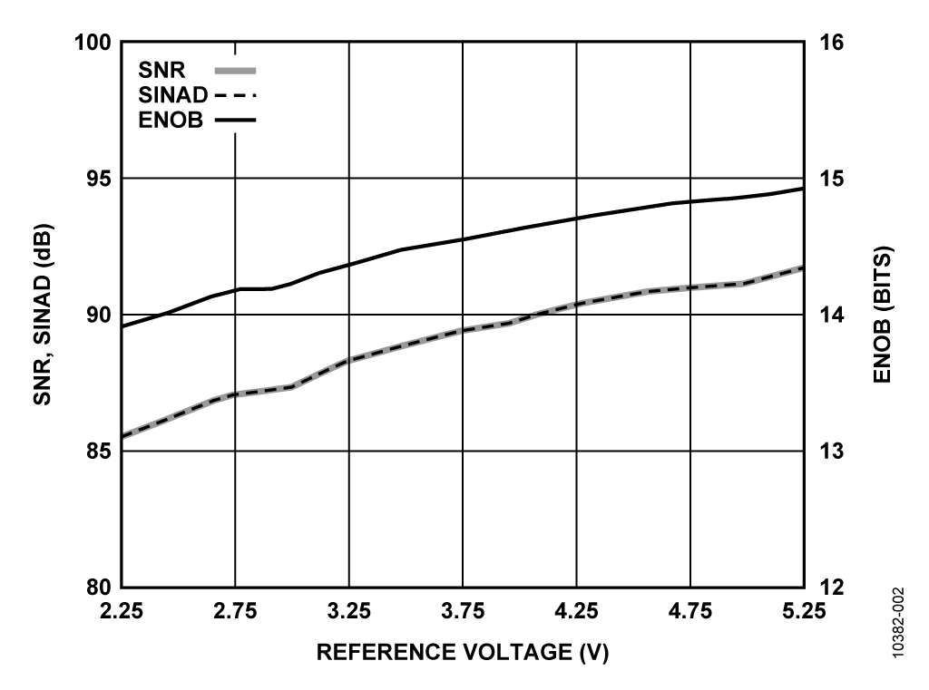
Measurement results for the circuit are shown in Figure 3. The SNR performance of 86.17 dB is comparable to that expected with the 2.5 V reference voltage, as previously shown in Figure 2.


Common Variations
Other pin-compatible, 16-bit ADCs in the PulSAR® family are available at higher sampling rates: AD7988-5 (500 kSPS), AD7980 (1 MSPS), and AD7983 (1.33 MSPS). Note that the higher sample rates require more power. Alternatively, if higher resolution is required, suitable pin-compatible devices are the AD7691 (18-bit, 250 kSPS), AD7690 (18-bit, 400 kSPS), AD7982 (18-bit, 1 MSPS differential input), and the AD7984 (18-bit, 1.33 MSPS).
For higher input voltage ranges, choose a higher voltage reference and higher voltage supply rails for both the reference and the ADC driver.
Dynamic performance is shown in Figure 4 for the AD7988-5 (16-bit, 500 kSPS) ADC under similar conditions; however, with a sampling rate of 500 kSPS. The SNR is equal to 86.37dB.


Adding an Input Common-Mode Voltage Bias Amplifier
In ac-coupled applications, the input signal must be biased so that it is centered within the ADC input range (0 V to 2.5 V for a 2.5 V reference). The circuit shown in Figure 5 addresses this common-mode signal requirement.
A wide range of amplifiers can be used for buffering purposes in this application. The AD8031 is a single-supply voltage feedback amplifier that features high speed performance with 80 MHz of small signal bandwidth, 30 V/μs slew rate, and 125 ns settling time. This amplifier is unity-gain stable with a capacitive load and consumes less than 2.5 mW of power from a single 3.3 V supply. The AD8031 is available in a 5-lead SOT-23, an 8-lead SOIC, an 8-lead PDIP, and an 8-lead MSOP. In this circuit, the AD8031 is used to buffer the 2.5 V voltage reference to a voltage divider that provides the required 1.25 V common-mode voltage to the input of the ADA4841-1. The additional power used by the buffer is shown in Table 2.


| Load | Description | Supply Current | Supply Voltage | Power |
| ADC | AD7988-1 | 150 µA | 2.5V | 375 µW |
| Driver | ADA4841-1 | 1.1 mA | 4V | 4.4 mW |
| Reference | ADR4525 | 600 µA | 4V | 2.4 mW |
| VCM Buffer | AD8031 | 750 µA | 4 V | 3 mW |
| Total | 10.17 mW |

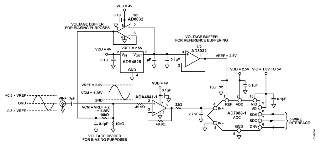
Adding a Reference Voltage Buffer
In applications where the voltage reference is shared between the different circuits, it may be necessary to buffer the reference voltage to ensure optimal performance. In this instance, using the AD8032 (a dual version of the AD8031) works quite nicely, as shown in Figure 6. Where the ADC reference input is buffered, the decoupling value can be reduced to a 10 ìF ceramic chip capacitor located as close to the device as possible.
Figure 7 and Figure 8 show the performance for both the AD7988-1 and the AD7988-5, respectively, when using the AD8032 amplifier to create the VCM voltage level and to buffer the reference voltage, as is shown in Figure 6. This is the circuit implemented on the EVAL-CN0255-SDPZ board.


Circuit Evaluation & Test
Equipment Needed (Equivalents Can Be Substituted)
- EVAL-CN0255-SDPZ
- System Demonstration Board (EVAL-SDP-CB1Z)
- Function generator/signal source, such as Audio Precision SYS-2522 used in these tests.
- Power supply, 2.5 V and 4 V
- PC with USB port, USB cable, and installed 10-lead PulSAR software
Setup and Test
The block diagram of the ac performance measurement setup is shown in Figure 9. Connect the 2.5 V and 4 V power supply to the evaluation board power terminal.
To measure the frequency response, connect the equipment as shown in Figure 9. Set the Audio Precision SYS-2522 signal generator for a 10 kHz frequency and a 2.5 V p-p sine wave with a 1.25 V dc offset. Record the data using the evaluation board software.
The software analysis is part of the evaluation board software that allows the user to capture and analyze ac and dc performance.

