LTC6951
最終販売超低ジッタ VCO内蔵の複数出力 クロック・シンセサイザ
- 製品モデル
- 4
- 1Ku当たりの価格
- 最低価格:$10.84
製品の詳細
- VCO内蔵の低ノイズ整数分周方式PLL
- 出力ジッタ:
- 90fs RMS (12kHz to 20MHz)
- 115fs RMS (ADC SNR 方式)
- ノイズフロア = –165dBc/Hz at 250MHz
- EZSync™、ParallelSync™ マルチチップ同期
- JESD204B/JESD204C、サブクラス1に適合するSYSREF生成
- 出力周波数範囲:
- 1.95MHz ~ 2.5GHz (LTC6951)
- 2.1MHz ~ 2.7GHz (LTC6951-1)
- 正規化された帯域内位相ノイズフロア:–229dBc/Hz
- 正規化された帯域内1/fノイズ:–277dBc/Hz
- 5 個の独立した低ノイズ出力
- リファレンス入力周波数:最大425MHz
- LTC6951Wizard™ソフトウェア設計ツールによるサポート
- 動作接合部温度範囲:–40°C~105°C
- LTC6951Wizard Design Tool
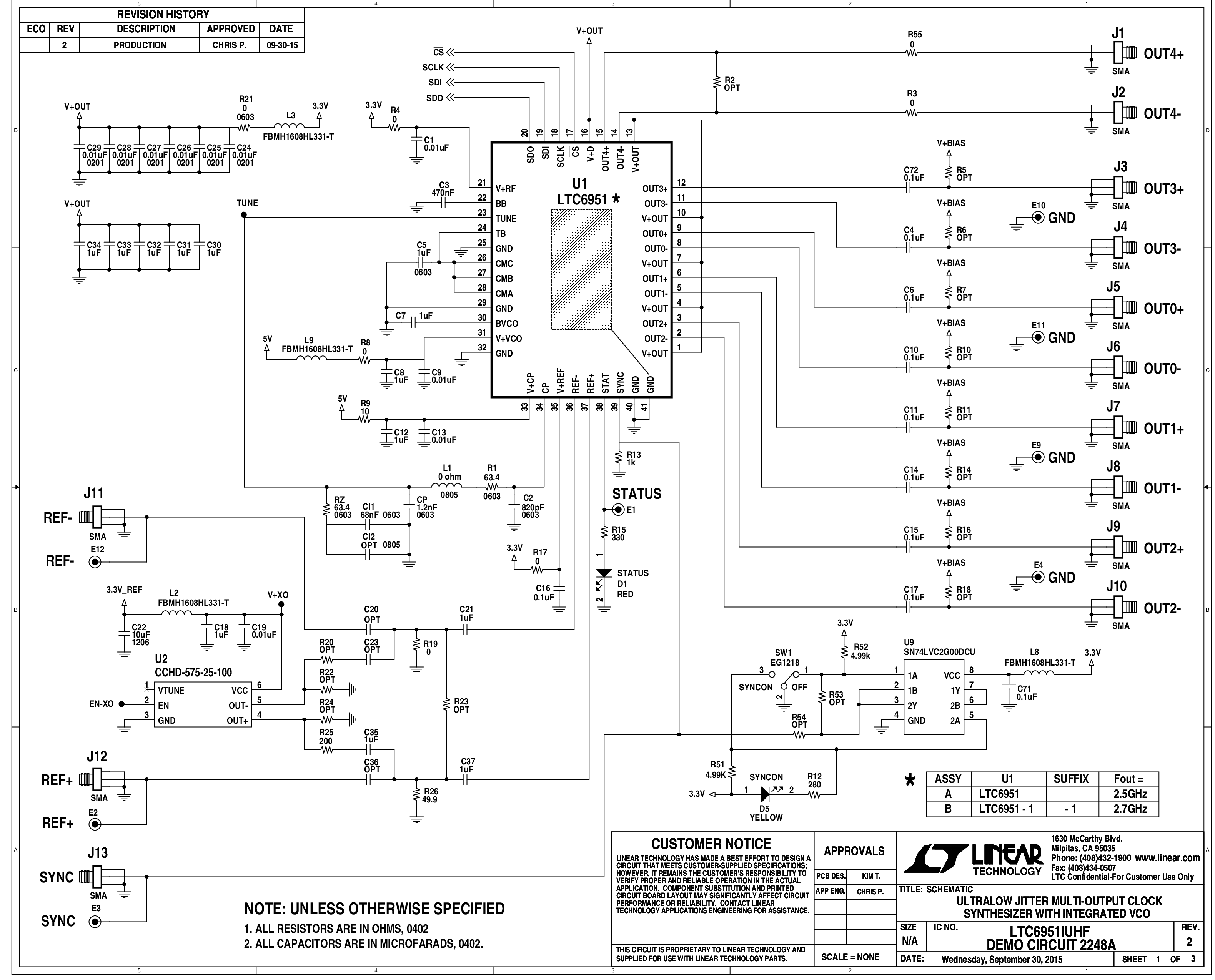
LTC6951は、VCOを完全に内蔵した高性能な低ノイズのフェーズロック・ループ(PLL)です。低ノイズVCOは、外部部品を必要とせず、外部システムのサポートがなくても正しい出力周波数に内部的に較正されます。
クロック生成セクションには、VCOプリスケーラ信号に基づいて5 個の出力が用意されており、出力ごとに個別分周器があります。4 個の出力は、超低ノイズでスキューの少ないCMLロジックを特徴としています。5 個目の出力は、低ノイズのLVDSです。これらの出力は全て、プログラム可能な遅延を使用して同期化し、正確な位相整列に設定できます。
目的の出力周波数が2.5GHz~2.7GHz、1.66GHz~1.8GHzまたは1.25GHz~1.35GHzの範囲内に収まる場合は、LTC6951-1を使用してください。他の全ての周波数の場合は、LTC6951を選択してください。
アプリケーション
- 高性能データ・コンバータ・クロッキング
- 無線インフラ
- テストおよび測定
ドキュメント
データシート 2
ユーザ・ガイド 2
アプリケーション・ノート 2
技術記事 1
プレス・リリース 1
製品セレクタ・カード 2
| 製品モデル | ピン/パッケージ図 | 資料 | CADシンボル、フットプリント、および3Dモデル |
|---|---|---|---|
| LTC6951IUHF#PBF | 40-Lead QFN (5mm x 7mm x 0.75mm w/ EP) | ||
| LTC6951IUHF#TRPBF | 40-Lead QFN (5mm x 7mm x 0.75mm w/ EP) | ||
| LTC6951IUHF-1#PBF | 40-Lead QFN (5mm x 7mm x 0.75mm w/ EP) | ||
| LTC6951IUHF-1#TRPBF | 40-Lead QFN (5mm x 7mm x 0.75mm w/ EP) |
| 製品モデル | 製品ライフサイクル | PCN |
|---|---|---|
|
3 20, 2024 - 23_0089 Obsolescence of Tower Fab3 (JAZZ-3) SBC35 Process |
||
| LTC6951IUHF#PBF | ||
| LTC6951IUHF#TRPBF | ||
| LTC6951IUHF-1#PBF | ||
| LTC6951IUHF-1#TRPBF | ||
これは最新改訂バージョンのデータシートです。
ソフトウェア・リソース
必要なソフトウェア/ドライバが見つかりませんか?
ドライバ/ソフトウェアをリクエストハードウェア・エコシステム
ツールおよびシミュレーション
Linduino 3
設計ツール 1
IBISモデル 1
Linduino はアナログ・デバイセズの Arduino 互換システムで、アナログ・デバイセズ製集積回路のファームウェア・ライブラリおよびサンプル・コードの開発と配布に使用します。Linduino対応の各製品には、LTSketchbook/Part Numberフォルダに定義されたサンプルのメイン・プログラムと、LTSketchbook/librariesフォルダに定義されたドライバ・コードが含まれています。
評価用キット

DC2430A Linduino SPI 1:8 Expander Demonstration Board (DC2026 Included)
資料
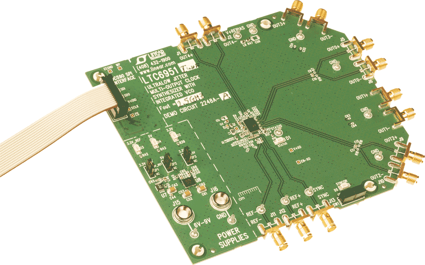
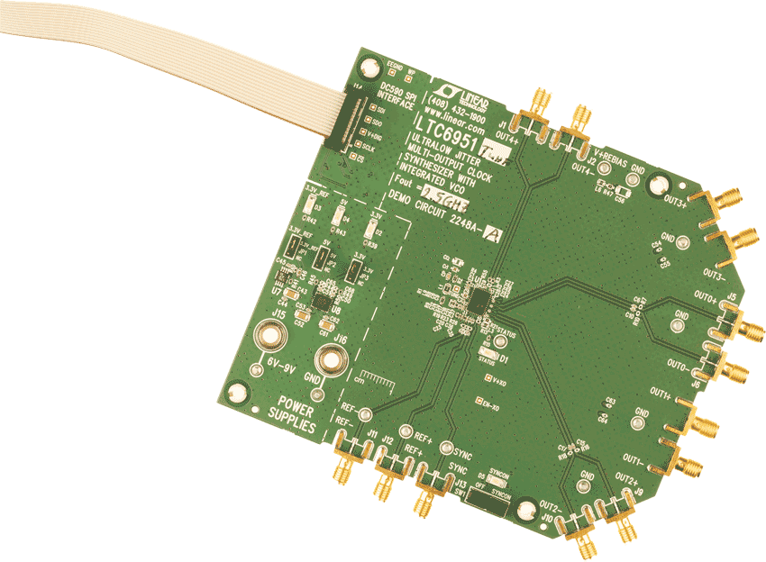
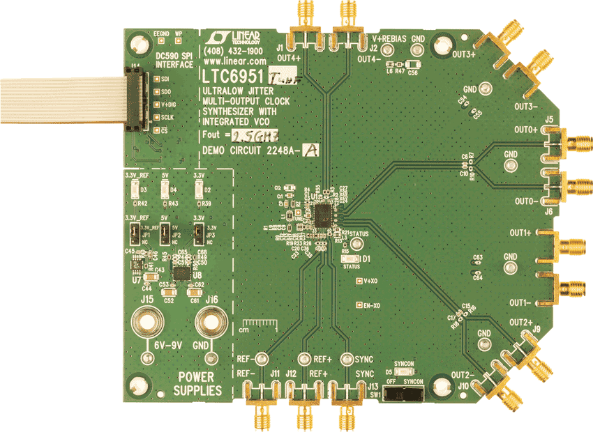
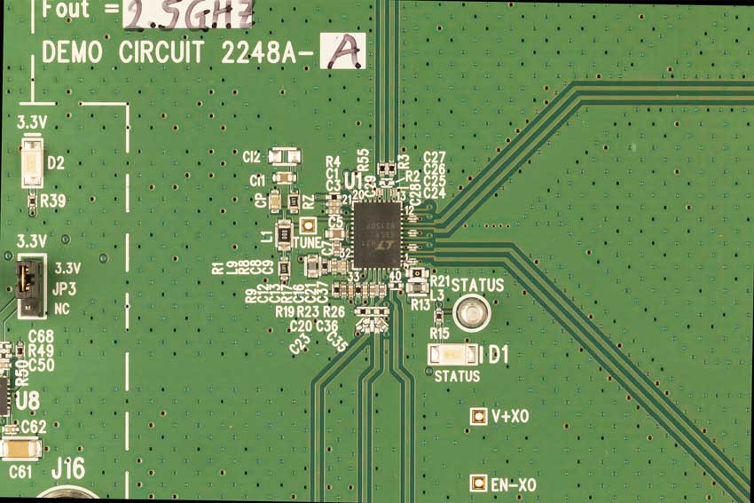
LTC6951 Demo Board | 5-Output Integer-N PLL with Integrated VCO, Output Range: 1.95MHz to 2.5GHz (requires DC590 or DC2026)
資料
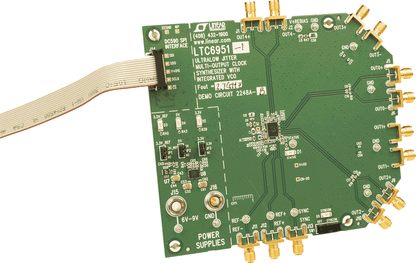
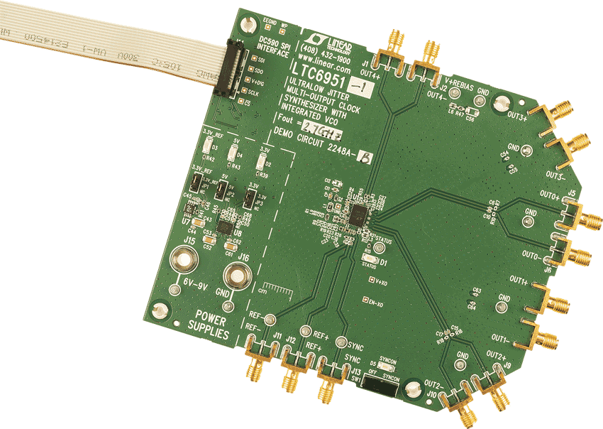
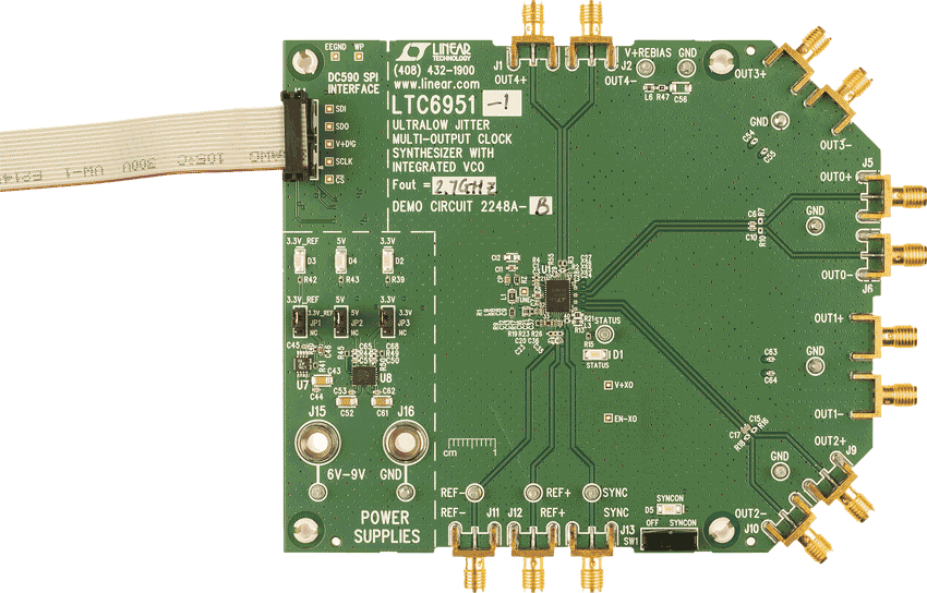
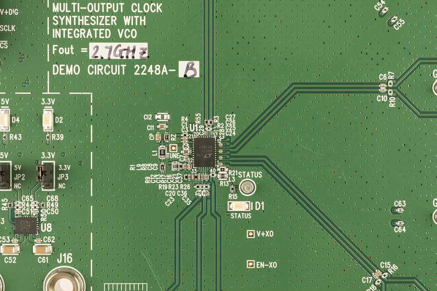
LTC6951-1 Demo Board | 5-Output Integer-N PLL with Integrated VCO, Output Range: 2.1MHz to 2.7GHz (requires DC590 or DC2026)
資料

4-Channel 14-Bit 250Msps JESD204B ADC with Clocking [Featuring LTC2123, LTC6951]