ADM7170
ADM7170
新規設計に推奨6.5V、500mA、超低ノイズ、高PSRR、高速過渡応答CMOS LDO
- 製品モデル
- 9
- 1Ku当たりの価格
- 最低価格:$1.13
Viewing:
製品の詳細
- 入力電圧範囲:2.3V~6.5V
- 最大負荷電流:500mA
- 低ノイズ:5μV(実効値、100Hz~100kHzで出力電圧に依存しない)
- 高速過渡応答:1.5μs(負荷ステップ1mA~500mA)
- 100kHz時に60dB PSRR
- 低ドロップアウト電圧:500mA負荷で42mV、VOUT = 3V
- 初期精度:±0.75%
- 電源ライン、負荷、温度に対する初期精度:±1.25%
- 静止電流、IGND = 0.7mA(負荷なし)
- 低シャットダウン電流:0.25μA(VIN = 5V)
- 小型4.7μFセラミック出力コンデンサで安定
- 可変出力電圧および固定出力電圧オプション:1.2V~5.0V
- 可変出力電圧素子の設定範囲:1.2V~VIN − VDO
- 高精度イネーブル
- 調整可能なソフト・スタート
- 8ピン3mm × 3mm LFCSPパッケージ
- ADIsimPowerツールのサポート
ADM7170は、2.3V~6.5Vで動作し、最大500mAの電流を出力するCMOS低ドロップアウト・リニア電圧レギュレータ(LDO)です。この高出力電流のLDOは、6V~1.2Vのレールを駆動する高性能アナログ回路やミックスド・シグナル回路を調整するのに最適です。当社独自の最新アーキテクチャを採用して高い電源変動除去比と低ノイズを実現しており、小型の4.7μFセラミック出力コンデンサを使うだけで、優れたライン過渡応答と負荷過渡応答を実現します。負荷過渡応答は1mA~500mAの負荷ステップで1.5μs(代表値)です。
ADM7170には、17の固定出力電圧のオプションがあります。以下の電圧の製品を標準在庫品として提供しています。1.3V、1.8V、2.5V、3.0V、3.3V、4.2V、および5.0V。その他の電圧は特注品として提供され、1.5V、1.85V、2.0V、2.2V、2.7V、2.75V、2.8V、2.85V、3.8V、および4.6Vを提供しています。1.2V~VIN − VDOの範囲の出力が可能な外付け帰還分圧器の付いた可変バージョンもご利用いただけます。
突入電流は、ソフト・スタート・ピンを使用して起動時間を調整することで制御できます。1nFソフト・スタート・コンデンサを使用したときの起動時間の代表値は約1.0msです。
ADM7170レギュレータの出力ノイズは、出力電圧に関係なく5μV(実効値)です。ADM7170は8ピン3mm × 3mmのLFCSPパッケージを採用しているため、非常に小型のソリューションが実現します。また、フットプリントが小さく、低プロファイルのパッケージで500mAまでの出力電流を必要とするアプリケーションに対して優れた熱性能も提供します。
アプリケーション
- 雑音の影響を受けやすいアプリケーションにおける電源レギュレーション:ADCおよびDAC回路、高精度アンプ、PLL/VCO、およびクロックIC
- 通信およびインフラストラクチャ
- 医療機器、健康機器
- 工業用機器、計測器
ドキュメント
データシート 2
ユーザ・ガイド 1
アプリケーション・ノート 1
ビデオ 2

ソリューション・カタログ 2
| 製品モデル | ピン/パッケージ図 | 資料 | CADシンボル、フットプリント、および3Dモデル |
|---|---|---|---|
| ADM7170ACPZ-1.3-R7 | 8-Lead LFCSP (3mm x 3mm w/ EP) | ||
| ADM7170ACPZ-1.8-R7 | 8-Lead LFCSP (3mm x 3mm w/ EP) | ||
| ADM7170ACPZ-2.5-R7 | 8-Lead LFCSP (3mm x 3mm w/ EP) | ||
| ADM7170ACPZ-3.0-R7 | 8-Lead LFCSP (3mm x 3mm w/ EP) | ||
| ADM7170ACPZ-3.3-R7 | 8-Lead LFCSP (3mm x 3mm w/ EP) | ||
| ADM7170ACPZ-4.2-R7 | 8-Lead LFCSP (3mm x 3mm w/ EP) | ||
| ADM7170ACPZ-5.0-R7 | 8-Lead LFCSP (3mm x 3mm w/ EP) | ||
| ADM7170ACPZ-R2 | 8-Lead LFCSP (3mm x 3mm w/ EP) | ||
| ADM7170ACPZ-R7 | 8-Lead LFCSP (3mm x 3mm w/ EP) |
| 製品モデル | 製品ライフサイクル | PCN |
|---|---|---|
|
2 25, 2025 - 25_0055 Gold Wire to Copper Wire Conversion(PCA) |
||
| ADM7170ACPZ-1.3-R7 | 製造中 | |
| ADM7170ACPZ-2.5-R7 | 製造中 | |
| ADM7170ACPZ-3.0-R7 | 製造中 | |
| ADM7170ACPZ-4.2-R7 | 製造中 | |
これは最新改訂バージョンのデータシートです。
ソフトウェア・リソース
必要なソフトウェア/ドライバが見つかりませんか?
ドライバ/ソフトウェアをリクエストハードウェア・エコシステム
| 製品モデル | 製品ライフサイクル | 詳細 |
|---|---|---|
| LT3045 | 新規設計に推奨 | 20V、500mA、超低ノイズ、超高PSRRのリニア・レギュレータ |
ツールおよびシミュレーション
LTspice
下記製品はLTspiceで使用することが出来ます。:
- ADM7170
- ADM7170-1.3
- ADM7170-1.8
- ADM7170-2.5
- ADM7170-3.0
- ADM7170-3.3
- ADM7170-4.2
- ADM7170-5.0
LTspice®は、無料で提供される強力で高速な回路シミュレータと回路図入力、波形ビューワに改善を加え、アナログ回路のシミュレーションを容易にするためのモデルを搭載しています。
評価用キット


RF Front-end GaN Power Amplifier Biasing, Protection, and Control Reference Design
資料
ソフトウェア
Evaluation System for the ADA4355
資料


Direct RF to Baseband Transmit Radio
資料

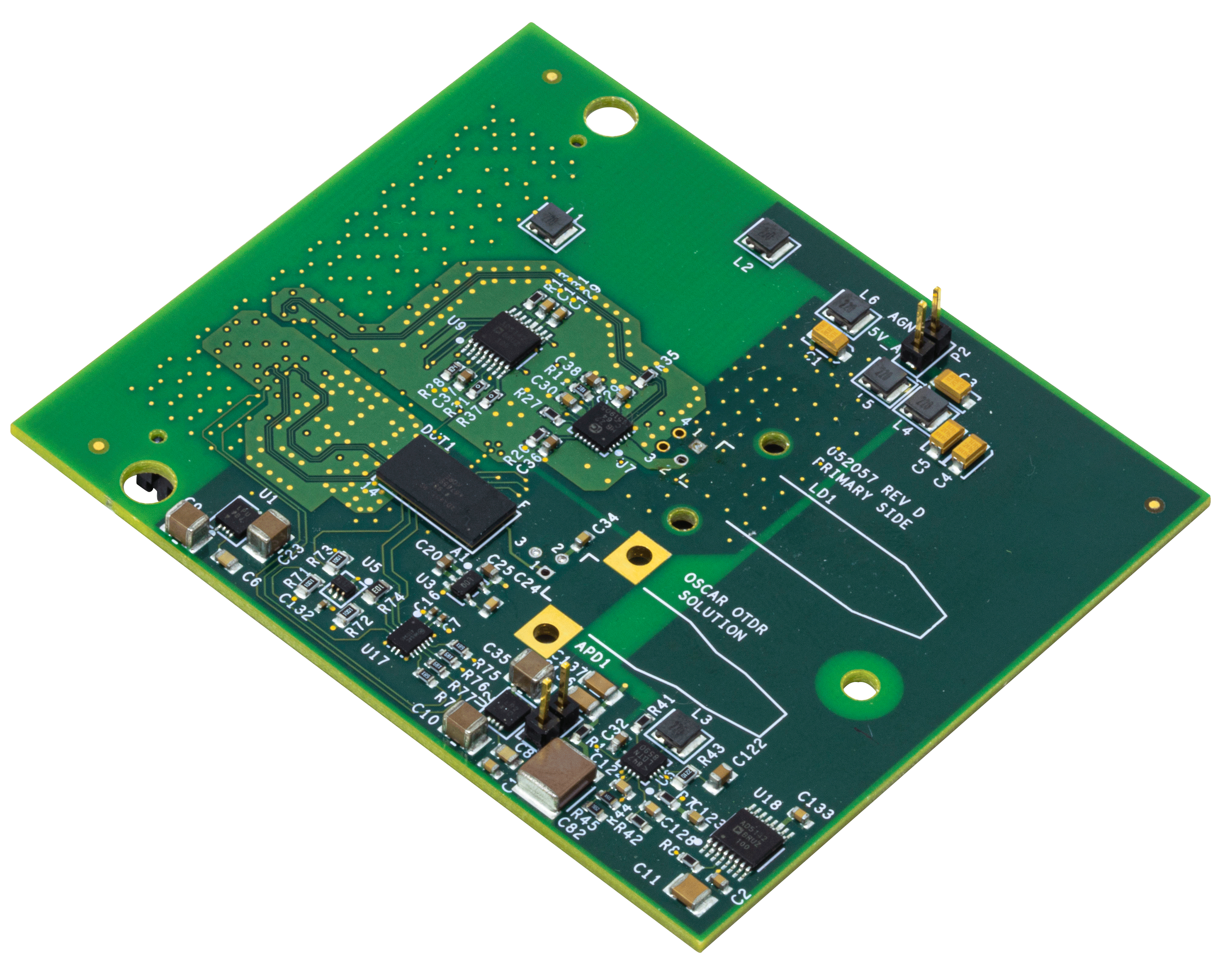
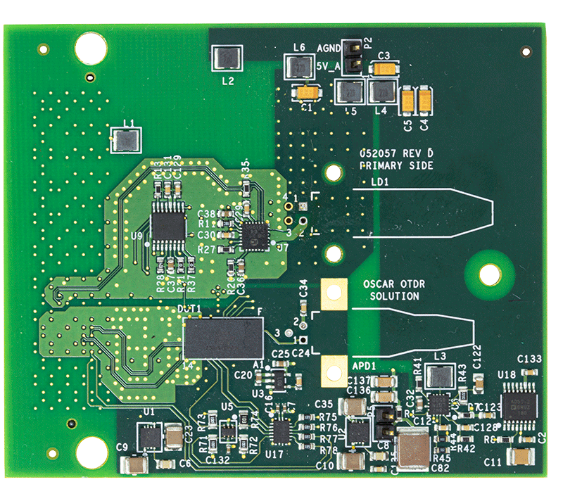
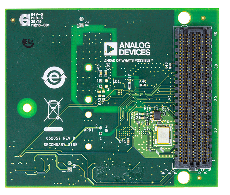
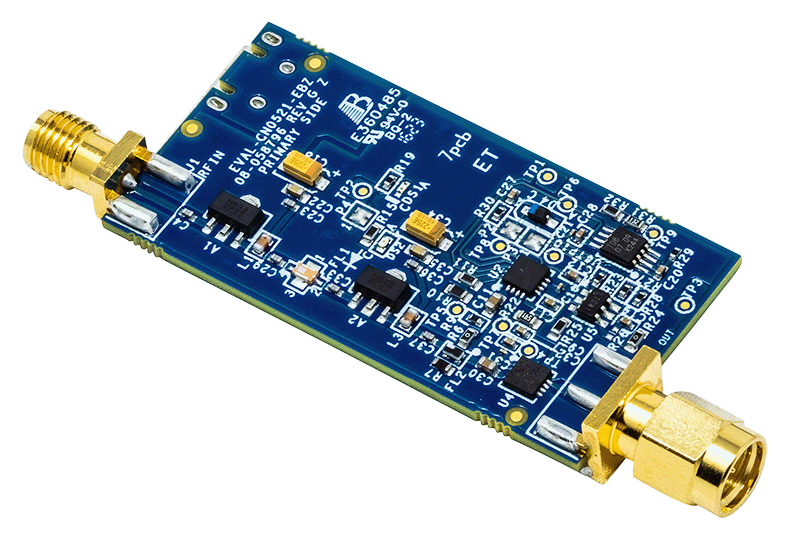
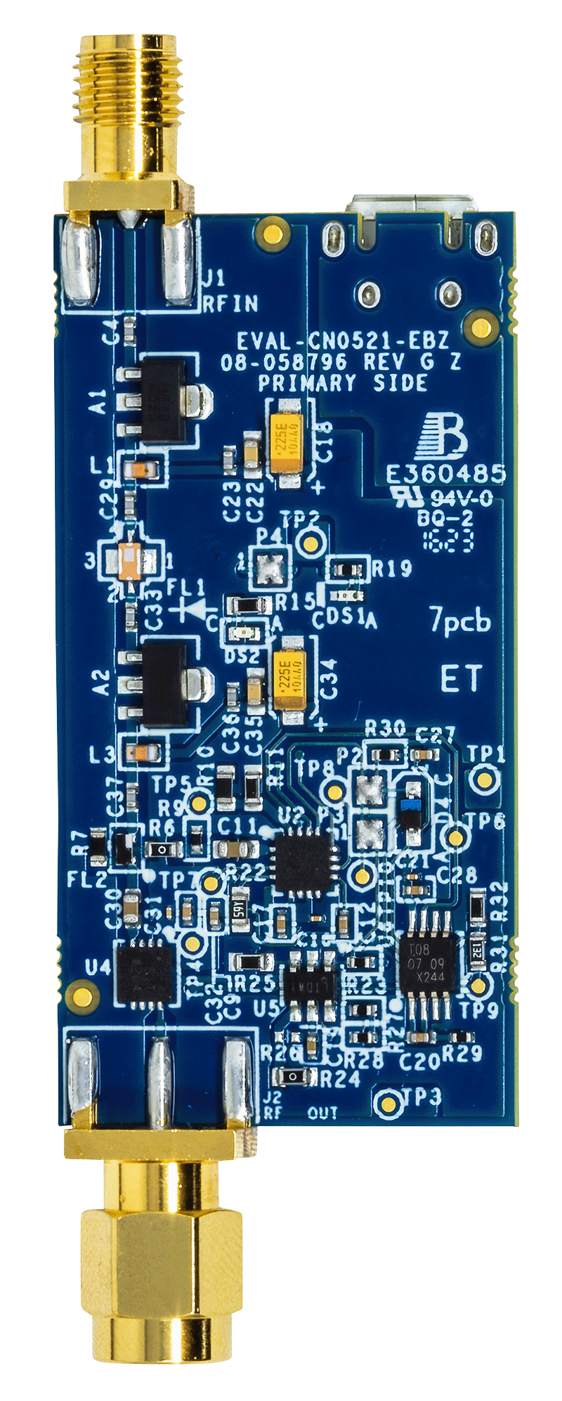
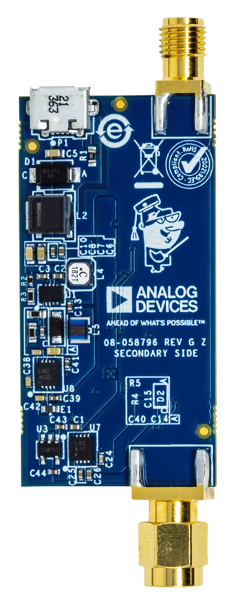
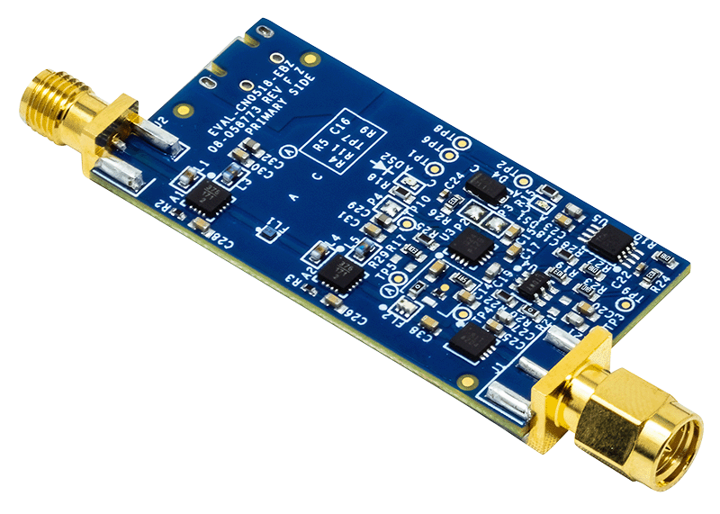
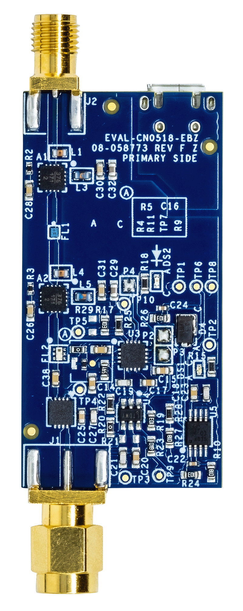
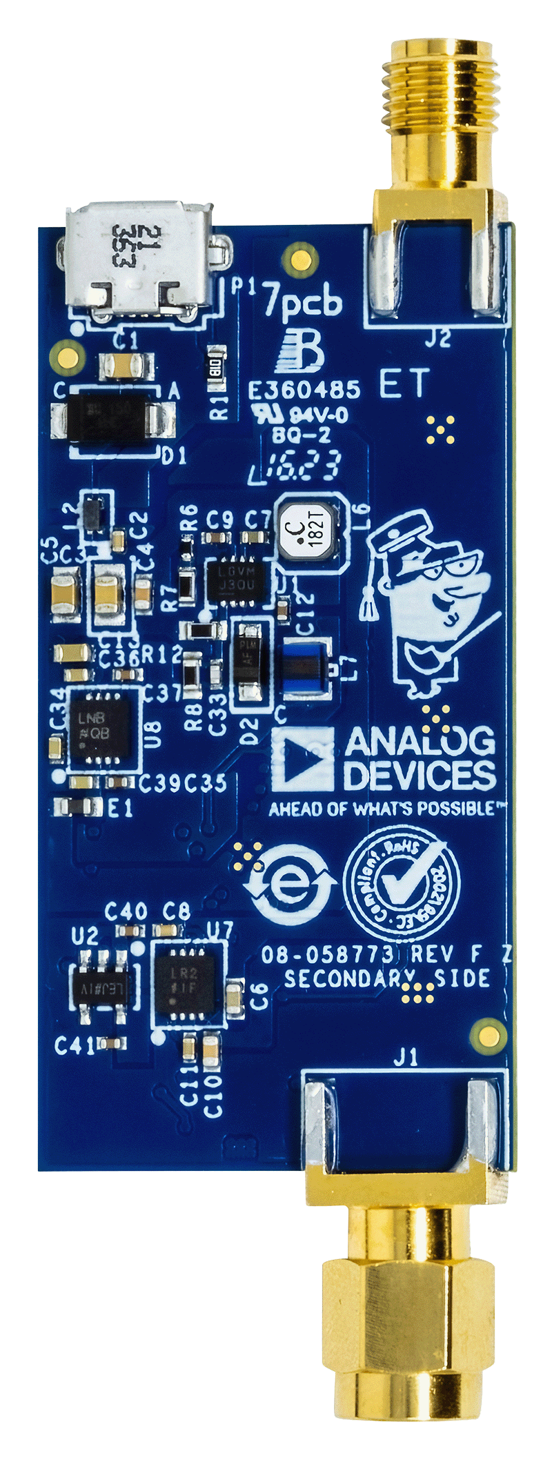
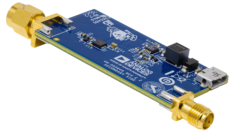
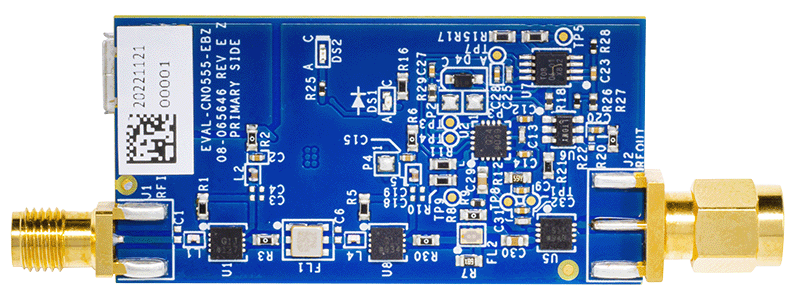
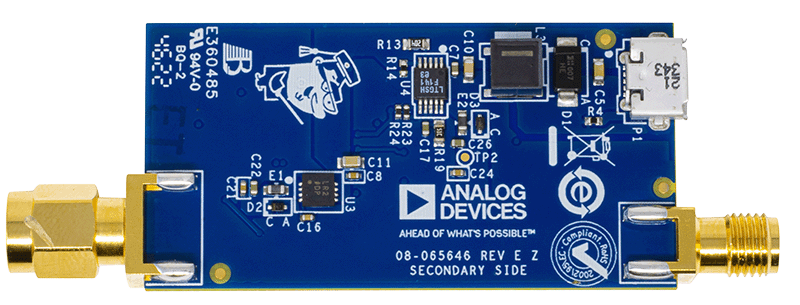
ADM7170/ADM7171/ADM7172評価用ボード
資料
リファレンス・デザイン
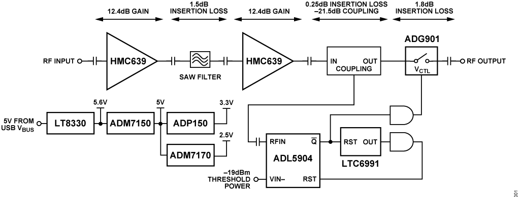
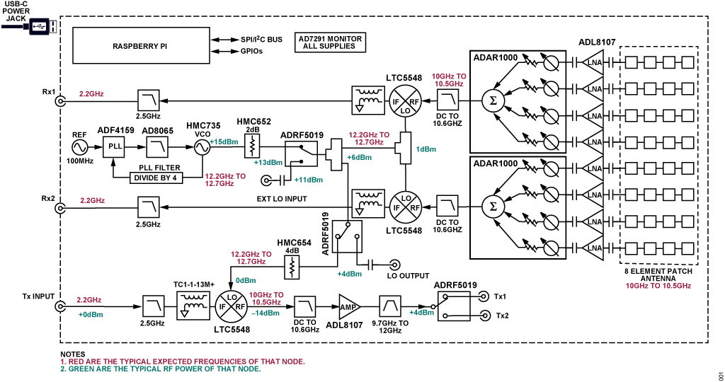
USB-Powered, 2.4 GHz RF Low Noise Amplifier Receiver with Overpower Protection Circuit
使用製品
設計および組み込みツール


フェーズド・アレイ開発プラットフォーム 開発入門ワークショップ開催中
使用製品
資料
設計および組み込みツール
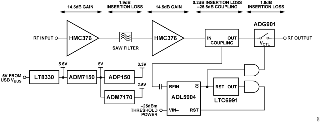
USB-Powered, 915 MHz RF Low Noise Amplifier Receiver with Overpower Protection Circuit
使用製品
設計および組み込みツール
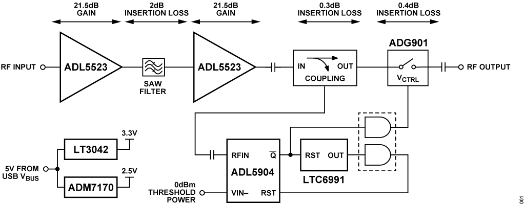
過電力保護機能を備えた、USB 駆動 433.92MHz RF 低ノイズ・アンプ・レシーバー