
智能工厂:IO-Link主站
IO-Link® is at the heart of the manufacturing revolution, with the IO-Link master as an intrinsic piece, bringing intelligence to the edge with its ability to transform traditional sensors into smart ones. IO-Link can help manufacturers bring their factories into the modern era without gutting and replacing their equipment. Acting as the brains of the operation, the IO-Link master brings flexibility and configurability to the factory floor by enabling self-commissioning sensors and actuators.
In the manufacturing environment, all manufactured products require an array of sensors working in unison to help machines determine distance to an object, detect the object, identify colors and composition of an object, as well as to monitor the temperature and pressure of the object. Analog Devices’ IO-Link helps manufacturers save on time and the most costly part of manufacturing floors by eliminating the need for sending technicians to the factory floor to manually change and recalibrate sensors. In making sensors and actuators self-commissioning and enabling bidirectional communication, our IO-Link technology optimizes the production line and streamlines the manufacturing flow.
Value and Benefits
The IO-Link master provides high-speed, bidirectional, digital data communication out to sensors and actuators at the very edge of the factory floor. This communication enables intelligence in both sensors and actuators, opening the door for new ways to measure, monitor, and influence every phase of the manufacturing line. Adding bidirectional communication abilities, IO-Link keeps sensors, actuators, and IO-Link gateways in constant communication with the main PLC. Real-time diagnostic information and updates allow engineers to identify and quickly address problems before they impact manufacturing flow. To connect the IO-Link master to the Ethernet network, our industrial Ethernet platform solution, the RapID Platform Generation 2 (RPG2), is pretested and certified for conformance to the industrial Ethernet protocol vendor’s test standards. A design using RPG2 will operate problem-free on any supported industrial Ethernet network, resulting in simplified development and reduced time to market.


Brings intelligence to the edge
Reduces factory downtime
Simplifies installation, interface, and Ethernet connectivity
MAX14819

MAX14819低功耗、双通道IO-Link®主机收发器带有传感器/执行器电源控制器,完全兼容最新IO-Link和二进制输入标准及测试规范IEC 61131-2、IEC 61131-9 SDCI和IO-Link 1.1.3。主机收发器也包括两路辅助数字输入(DI_)通道。
MAX14819可配置为配合外部UART工作,或者使用IC上的集成成帧器。
为便于选择微控制器,主机收发器具有帧处理电路,… 更多...
MAX14819低功耗、双通道IO-Link®主机收发器带有传感器/执行器电源控制器,完全兼容最新IO-Link和二进制输入标准及测试规范IEC 61131-2、IEC 61131-9 SDCI和IO-Link 1.1.3。主机收发器也包括两路辅助数字输入(DI_)通道。
MAX14819可配置为配合外部UART工作,或者使用IC上的集成成帧器。
为便于选择微控制器,主机收发器具有帧处理电路,带有UART和FIFO。器件设计用于简化所有IO-Link M序列帧类型的时间关键控制。MAX14819也具有自主循环定时器,降低对高精度控制器时序的要求。集成建立通信排序器也简化唤醒管理。
MAX14819集成两个低功耗传感器电源控制器,具有高级限流、反向电流保护和极性反接保护能力,支持低功耗可靠方案。
MAX14819采用48引脚(7mm × 7mm) TQFN封装,工作在-40°C至+125°C扩展级温度范围。

应用
- IO-Link网关
- IO-Link主机系统
应用
MAX14916

MAX14916 具有八个高压端开关,每通道可提供高达 1.1A(最小值)连续电流。两个相邻通道可以并联,从而构成四个 2.4A 高压端开关。在 125°C 环境温度下,高压端开关具有 250mΩ(最大值)的导通电阻。
SPI 接口具有内置芯片寻址解码器,从而允许利用公共 SPI 芯片选择与多个 MAX14916 通信(低温启动 CS 引脚被拉低)。 SPI 接口为全局和每个通道的配置和诊断提供了… 更多...MAX14916 具有八个高压端开关,每通道可提供高达 1.1A(最小值)连续电流。两个相邻通道可以并联,从而构成四个 2.4A 高压端开关。在 125°C 环境温度下,高压端开关具有 250mΩ(最大值)的导通电阻。
SPI 接口具有内置芯片寻址解码器,从而允许利用公共 SPI 芯片选择与多个 MAX14916 通信(低温启动 CS 引脚被拉低)。 SPI 接口为全局和每个通道的配置和诊断提供了灵活性,包括欠压检测、明线/负载检测、过载和电流限制报告、热状况报告等。 开路负载检测可利用开启和关闭状态的开关检测明线/开路负载状况。LED 驱动器可按通道提供故障、状态以及电源欠压状况指示。用于快速关闭电感负载的内部有源钳位 在 VDD 上,集成的线对地和线对线浪涌保护仅需要一个 TVS。集成的浪涌保护对四路和八路配置均有效。 MAX14916 采用紧凑的 48 引脚 6mm x 6mm QFN 封装。应用
- 工业数字输出
- PLC 系统
应用
ADIN2299

ADIN2299 是一款经过预先测试的完整解决方案,用于管理应用处理器的工业协议和网络流量。
该模块包含部署实施Ether-CAT、PROFINET®实时(RT)和同步实时(IRT)、EtherNet/IP网络所需的一切,包括通信控制器、协议栈、闪存、RAM、跟随器控制器和物理层(PHY)。应用处理器通过通用异步接收器发送器(UART)、串行外设接口(SPI)或以太网接口进行连接。
在软件层,应… 更多...
ADIN2299 是一款经过预先测试的完整解决方案,用于管理应用处理器的工业协议和网络流量。
该模块包含部署实施Ether-CAT、PROFINET®实时(RT)和同步实时(IRT)、EtherNet/IP网络所需的一切,包括通信控制器、协议栈、闪存、RAM、跟随器控制器和物理层(PHY)。应用处理器通过通用异步接收器发送器(UART)、串行外设接口(SPI)或以太网接口进行连接。
在软件层,应用处理器连接到统一接口,因此可以在不更改应用处理器软件的情况下使用支持的工业协议。ADIN2299平台经过预认证,因此现场设备可以在任何受支持的工业以太网中运行。
产品特色
- 多协议支持
- 小尺寸支持嵌入式应用
- 用于具有独特形状因子的应用程序的嵌入式设计解决方案
- 低功耗、低延迟
- 强大的网络监管确保符合PROFINET网络负载3类要求
应用
- 工厂和过程自动化
- 运动控制
- 楼宇自动化
- 交通运输
- 机器人
- 能量
应用
能源解决方案
- 智能电网基础设施解决方案
- 继电保护(电力线路监控)
智能楼宇解决方案
- 楼宇自动化系统
- 楼宇安全和安保解决方案
MAXM15065

喜马拉雅系列稳压器IC和电源模块提供低温升、小尺寸、较简单的电源方案。MAXM15465/MAXM15466/MAXM15065/MAXM15066/MAXM15067为高效、同步降压型DC-DC电源模块系列,集成控制器、MOSFET、补偿元件和电感,工作在较宽输入电压范围。模块工作在4.5V至60V输入电压范围,提供高达300mA输出电流。MAXM15065和MAXM15066分别为3.3V和5… 更多...
喜马拉雅系列稳压器IC和电源模块提供低温升、小尺寸、较简单的电源方案。MAXM15465/MAXM15466/MAXM15065/MAXM15066/MAXM15067为高效、同步降压型DC-DC电源模块系列,集成控制器、MOSFET、补偿元件和电感,工作在较宽输入电压范围。模块工作在4.5V至60V输入电压范围,提供高达300mA输出电流。MAXM15065和MAXM15066分别为3.3V和5V固定输出模块。
MAXM15067为可调节输出(0.9V至6.3V)模块。模块大大降低设计复杂度、制造风险,提供真正的即插即用电源方案,缩短上市时间。
MAXM15065/MAXM15066/MAXM15067模块采用峰值电流模式控制方法。为降低输入浪涌电流,模块提供3.75ms固定软启动时间。
MAXM15065/MAXM15066/MAXM15067模块采用薄型、小尺寸、10引脚、2.6mm x 3mm x 1.5mm、µSLIC ™封装。
应用
- 工业传感器和编码器
- 4–20mA电流环路供电传感器
- 替代LDO
- HVAC与楼宇控制
- 电池供电设备
- 通用负载点
- USB Type-C供电负载
应用
MAX32670

在Darwin家族中,MAX32670是一款超低功耗、高性价比、高可靠性的32位微控制器,在实现复杂的传感器处理设计的同时不会影响电池寿命。器件集成了高度灵活性的多功能电源管理单元与功能强大的Arm® Cortex®-M4 (带浮点运算单元,FPU)。MAX32670也为传统设计从8或16位微控制器升级提供了简便、成本优化的途径。
器件集成高达384KB闪存和160KB SRAM承载应用程序和传… 更多...
在Darwin家族中,MAX32670是一款超低功耗、高性价比、高可靠性的32位微控制器,在实现复杂的传感器处理设计的同时不会影响电池寿命。器件集成了高度灵活性的多功能电源管理单元与功能强大的Arm® Cortex®-M4 (带浮点运算单元,FPU)。MAX32670也为传统设计从8或16位微控制器升级提供了简便、成本优化的途径。
器件集成高达384KB闪存和160KB SRAM承载应用程序和传感器代码。在整个闪存、RAM和缓存全领域内支持纠错码(ECC),支持单比特纠错和双比特检测(SEC-DED),确保超高可靠性的代码执行支持一些要求苛刻的应用。另外集成了一些附加功能,例如集成了两个窗型看门狗定时器,具有极高的灵活性和独立时钟,进一步增强了方案的可靠性。掉电检测功能确保掉电、上电以及意外电源瞬变期间系统的正确工作。
器件集成了多种高速外设,例如3.4MHz I²C、50MHz SPI和4MBAUD UARTs,最大程度提高通信带宽。此外,提供一个低功耗UART可在最低功耗休眠模式下运行,促进唤醒而避免丢失任何数据。提供总共6个具有I/O功能的定时器,包括2个低功耗定时器,即使在最低功耗休眠模式下也可以进行脉冲计数、捕获/比较和PWM。该器件将全部这些功能集成到微小尺寸封装中:5mm x 5mm、40引脚TQFN-EP封装和1.7mm x 2.2mm、24焊球WLP封装。
应用
- 算法协处理器
- 电池供电医疗设备
- 工业传感器
- 光通信模块
- 安全无线电调制解调器控制器
- 智能传感器控制器
- 系统辅助功能控制器
应用
能源解决方案
- 智能仪表技术
医疗健康解决方案
- 适合医疗健康的治疗设备解决方案
- 活动跟踪和跌倒检测解决方案
- 呼吸率测量
- 心电图 (ECG) 测量
- 可穿戴健康监护仪
- 血氧饱和度 (SpO2) 测量
智能楼宇解决方案
- 烟雾探测
- 安防和监控
- 楼宇自动化控制器和网络解决方案
MAX22514

MAX22514 IO-Link收发器集成高压功能,包括一个24V线路驱动器、一个集成式DC-DC降压稳压器,以及5V和3.3V线性稳压器。MAX22514适用于IO-Link器件、主机和工业开关传感器应用,可以通过标准SPI接口进行配置和监控。
应用
- IO-Link、工业传感器和驱动器器件
- MAX22514采用SPI接口来进行配置和诊断。高度集成(包括2 … 更多...
MAX22514 IO-Link收发器集成高压功能,包括一个24V线路驱动器、一个集成式DC-DC降压稳压器,以及5V和3.3V线性稳压器。MAX22514适用于IO-Link器件、主机和工业开关传感器应用,可以通过标准SPI接口进行配置和监控。
应用
- IO-Link、工业传感器和驱动器器件
- MAX22514采用SPI接口来进行配置和诊断。高度集成(包括2个线性稳压器、一个DC-DC降压稳压器、集成式浪涌保护、低功耗散热和小型封装)使MAX22514实现优化,能够用于多种不同的工业和IO-Link小型传感器应用中。
- IO-Link主机收发器:MAX22514能够用于IOLink器件和IO-Link主机应用中。SPI接口用于实现扩展配置和诊断,收发器可以按照COM1、COM2和COM3 IO-Link数据速率运行。MAX22514经过配置,可以在C/Q电路中实现所需的5mA下拉/上拉电流,并生成唤醒脉冲。
应用
MAX32670EVKIT

MAX32670评估套件(EV kit)为评估MAX32670提供平台。MAX32670是一款超低功耗、高性价比、高可靠性32位微控制器,在实现复杂的传感器处理设计的同时不会影响电池寿命。器件集成了高度灵活性的多功能电源管理单元与功能强大的Arm® Cortex®-M4核心(带浮点运算单元,FPU)。MAX32670也为传统设计从8或16位微控制器升级提供了简便、成本优化的途径。
应用
- 算法协处理器
- 电 … 更多...
MAX32670评估套件(EV kit)为评估MAX32670提供平台。MAX32670是一款超低功耗、高性价比、高可靠性32位微控制器,在实现复杂的传感器处理设计的同时不会影响电池寿命。器件集成了高度灵活性的多功能电源管理单元与功能强大的Arm® Cortex®-M4核心(带浮点运算单元,FPU)。MAX32670也为传统设计从8或16位微控制器升级提供了简便、成本优化的途径。
应用
- 算法协处理器
- 电池供电医疗设备
- 工业传感器
- 光通信模块
- 安全无线电调制解调器控制器
- 智能传感器控制器
- 系统辅助功能控制器
相关产品
MAX32670
高可靠性、超低功耗微控制器,采用Arm Cortex M4 FPU处理器,适用于工业和IoT
应用
能源解决方案
- 智能仪表技术
医疗健康解决方案
- 适合医疗健康的治疗设备解决方案
- 活动跟踪和跌倒检测解决方案
- 呼吸率测量
- 心电图 (ECG) 测量
- 可穿戴健康监护仪
- 血氧饱和度 (SpO2) 测量
智能楼宇解决方案
- 烟雾探测
- 安防和监控
- 楼宇自动化控制器和网络解决方案
MAXREFDES145

The MAXREFDES145# is a fully IO-Link®-compliant, 8-port IO-Link master reference design. This design uses TEConcept's IO-Link master stack and is both an IO-Link master reference design as well as an… 更多...
The MAXREFDES145# is a fully IO-Link®-compliant, 8-port IO-Link master reference design. This design uses TEConcept's IO-Link master stack and is both an IO-Link master reference design as well as an IO-Link sensor/actuator development and test system. Eight IO-Link ports allow for simultaneous testing of up to eight different sensors (or actuators). The reference design has eight robust female M12 connectors, the most common connector used for IO-Link, and ships with two IO-Link cables to quickly connect to IO-Link compatible sensors and actuators. An AC-to-DC (24VDC/1A) power-supply cube is capable of providing at least 125mA simultaneously to each port and more when fewer ports are unused. A USB 2.0 Type B connector allows for quick connectivity to a Windows® PC.
The easy-to-use TEConcept Control Tool (CT) GUI software with IODD file import capability makes the MAXREFDES145# a must-have for any company or engineer serious about developing IO-Link products.
收起...相关产品
MAX14819
双通道IO-Link主机收发器,集成成帧器和L+电源控制器
MAX15062
60V、300mA、超小尺寸、高效、同步降压型DC-DC转换器
MAX14931
四通道、 1kVRMS、2.75kVRMS及3.75kVRMS数字隔离器
MAX12931
双通道数字隔离器
MAX15006
40V、超低静态电流线性稳压器,6引脚TDFN/8引脚SO封装
MAX4402
单/双/四路、低成本、单电源、满摆幅运算放大器,带有关断
应用
MAXREFDES165

相关产品
应用
MAXREFDES277
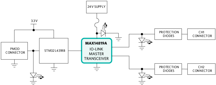
The MAXREFDES277# is a dual-channel IO-Link® master reference design optimized for quick prototyping. This design uses the Technologie Management Gruppe (TMG TE) IO-Link master stack for the MAX14819… 更多...
The MAXREFDES277# is a dual-channel IO-Link® master reference design optimized for quick prototyping. This design uses the Technologie Management Gruppe (TMG TE) IO-Link master stack for the MAX14819A IO-Link master transceiver and is both an evaluation model for an IO-Link master as well as an IO-Link sensor/actuator development and test system. Two IO-Link ports allow for simultaneous testing of up to two different sensors or actuators.
In this design, an STM32™ low-power microcontroller interfaces between the MAX14819A and the control board. The MAX14819A is a dual-channel IO-Link master transceiver with integrated framers and L+ supply controllers. Integrated L+ controllers are used to supply power to connected IO-Link devices. The MAX14819A integrated IO-Link framer offloads time-critical tasks from the microcontroller, easing prototyping and software requirements.
Peripheral module (Pmod™) interface is an open standard written by Digilent, Inc., and is typically used for quick development and prototyping. The MAXREFDES277# with its Pmod and non-standard IO-Link connectors is optimized for this type of functionality. In lieu of the standard M12 connectors used in IO-Link, the MAXREFDES277# uses two small on-board connectors with L+, L-, and IO-Link connections to maintain a small size board.
The board ships with two M12-to-wire IO-Link cables required to connect IO-Link devices (e.g., sensors and/or actuators) to the MAXREFDES277# master board. An AC-to-DC (24V DC/1A) power supply, capable of providing the 24V power to the on-board MAX14819A IO-Link master transceiver and any connected sensors or devices, is also included.
Connecting the MAXREFDES277# to any Analog Devices, Inc., IO-Link device reference design, with the associated software, allows for easy evaluation.
Design files and sample MicroPython software are available in the Design Files. The board is also available for purchase.
收起...应用
MAXREFDES42

概述
MAXREFDES42是一款高精度IO-Link®电阻温度检测器(RTD)温度传感器参考设计,可在较宽的温度范围内与2线、3线或4线PT100 RTD配合使用。该设计基于工业外形尺寸,采用Maxim Integrated的高集成度MAX31865 RTD数字转换器。通过坚固耐用的板载M12插口连接器,使用标准M12延长线即可将现成的RTD连接到电路板。温度传感器可将温度精确转换为15位分辨率… 更多...
概述
MAXREFDES42是一款高精度IO-Link®电阻温度检测器(RTD)温度传感器参考设计,可在较宽的温度范围内与2线、3线或4线PT100 RTD配合使用。该设计基于工业外形尺寸,采用Maxim Integrated的高集成度MAX31865 RTD数字转换器。通过坚固耐用的板载M12插口连接器,使用标准M12延长线即可将现成的RTD连接到电路板。温度传感器可将温度精确转换为15位分辨率,并具有多种故障检测功能。显示屏将显示近似温度(四舍五入到°C),而IO-Link通信则跟踪并提供更准确的温度值。该传感器利用IQ2 Development的IO-Link器件协议栈与任何IO-Link版本1.1兼容主机进行通信。该参考设计采用工业DC-DC降压转换器,功耗很低。该板还包含M12插头连接器,可使用标准M12电缆连接到兼容的IO-Link主机。将MAXREFDES42#连接到USB IO-link主机(例如IQ2 Development iqInterface® IO-Linkk主机),使用iqTool®软件可通过PC进行评估。
有关实验室测量数据的更多信息,请参阅“详情”标签页。设计文件和固件可从“设计资源”标签页下载。
收起...MAXREFDES37

The MAXREFDES37 IO-Link servo driver provides 5V power, four PWM outputs and four digital inputs for control of up to four 5V servo motors. IO-Link offers the ability to replace pneumatic actuators,… 更多...
The MAXREFDES37 IO-Link servo driver provides 5V power, four PWM outputs and four digital inputs for control of up to four 5V servo motors. IO-Link offers the ability to replace pneumatic actuators, and their compressed air lines, in industrial applications. With added level translation, the digital inputs allow for interfacing to binary position or status sensors. This design unveils a completely new application to the industrial segment with potential to disrupt the traditional pneumatic methods used today.
Onboard, standard 3-pin headers allow quick connection to off-the-shelf 5V servo motors. The MAXREFDES37 comes with a HiTec HS-53 servo motor. Push-in terminal blocks allow simple connection to 5V digital inputs, power, ground, and also access to all four PWM channels. The onboard rugged male M12-4 connector allows for a standard connection to any compliant IO-Link master. The MAXREFDES37 utilizes Technologie Management Gruppe Technologie und Engineering’s (TMG TE) IO-Link device stack. Maxim Integrated recommends using the MAXREFDES79 IO-Link master with simple-to-use graphical user interface (GUI) program for easy verification using a Windows® PC.
收起...MAXREFDES164

Overview
The MAXREFDES164# is a complete, high-accuracy, IO-Link®, local temperature sensor reference design that provides excellent temperature accuracy from -20°C to +105°C. Built in an industrial… 更多...
Overview
The MAXREFDES164# is a complete, high-accuracy, IO-Link®, local temperature sensor reference design that provides excellent temperature accuracy from -20°C to +105°C. Built in an industrial form factor, the design makes use of Maxim’s highly integrated MAX31875 digital temperature sensor with an I2C interface.
The MAX31875 operates over the -50°C to +150°C temperature range and measures temperatures from -40°C to +145°C with ±1.5°C accuracy. The temperature sensor performs more accurate temperature conversions from 0°C to +70°C (±1.0°C).
A MAX32660 microcontroller interfaces between the MAX31875 temperature sensor and the MAX14828 IO-Link® device transceiver. All three Maxim products are in wafer-level packages (WLPs), allowing the MAXREFDES164# to have a tiny footprint—under an inch in length. The 3.3V and 5V rails are generated by utilizing the two integrated LDO regulators within the MAX14828, which saves external components and space. In addition, the three Maxim ICs are low-power devices, allowing this reference design to consume minimal power with low thermal dissipation.
This sensor utilizes either the TMG TE IO-Link device stack or the TEConcept IO-Link device stack to communicate with any IO-Link version 1.1-compliant master. The board contains a male M12 connector for connection to a compliant IO-Link master using a standard M12 cable. Connecting the MAXREFDES164# to a USB IO-link master, such as the MAXREFDES165#, with the associated software allows for easy evaluation with a PC.
Note: The default stack that ships with the MAXREFDES164# is the TMG version. Contact the factory if you require the TEConcept version.
Design files, firmware, and software can be found on the Design Resources tab. The board is also available for purchase.
收起...MAXREFDES173

The MAXREFDES173# is a complete, high-accuracy, IO-Link®, local temperature sensor reference design that provides excellent temperature accuracy from -40°C to +85°C. Built in an industrial form… 更多...
The MAXREFDES173# is a complete, high-accuracy, IO-Link®, local temperature sensor reference design that provides excellent temperature accuracy from -40°C to +85°C. Built in an industrial form factor, the design makes use of the ADI MAX31875 digital temperature sensor with an I2C interface.
The MAX31875 operates over the −50°C to +150°C temperature range and measures temperatures from −40°C to +145°C with an accuracy of ±1.75°C or better. The temperature sensor performs more accurate temperature conversions from 0°C to +70°C (±1.0°C).
A Renesas RL78 (R5F10E8EALA) microcontroller interfaces between the MAX31875 temperature sensor and the MAX14827A IO-Link device transceiver. The RL78 microcontroller operates from −40°C to +85°C. The 3.3V and 5V rails are generated by two integrated LDO regulators within the MAX14827A, which reduces the number of required external components and the required circuit footprint. Both the MAX31875 and the MAX14827A are low-power devices, which allow this reference design to consume minimal power with low thermal dissipation. Additionally, both ADI products are in wafer-level packages (WLPs), giving the MAXREFDES173# a tiny overall footprint.
This sensor utilizes the IQ2 Development™ IO-Link device stack to communicate with any IO-Link version 1.1-compliant master. The board contains a male M12 connector for connection to a compliant IO-Link master using a standard M12 cable. Connect the MAXREFDES173# to any IO-link master for easy evaluation (for example, the iqLink® USB IO-Link Master with the associated software).
Design files, firmware, and software are available on the Design Resources tab. The board is also available for purchase.
收起...MAXREFDES163

The MAXREFDES163# is one of the world’s smallest industrial magnetic sensor solutions that uses a RedRock™ RR120 TMR integrated digital magnetic sensor and the MAX14839, an industrial sensor output.… 更多...
The MAXREFDES163# is one of the world’s smallest industrial magnetic sensor solutions that uses a RedRock™ RR120 TMR integrated digital magnetic sensor and the MAX14839, an industrial sensor output.
The reference design PCB dimension is just 15mm long × 10mm wide, with the width determined by the size of the M12 connector.
Design files can be found on the Design Resources tab. The board is also available for purchase.
收起...MAXREFDES171

Introduction
Advanced factory automation solutions, such as Industry 4.0, require increasing numbers of smart sensors, which are typically controlled using IO-Link® for the point-to-point serial… 更多...
Introduction
Advanced factory automation solutions, such as Industry 4.0, require increasing numbers of smart sensors, which are typically controlled using IO-Link® for the point-to-point serial communication between the sensor and controller (master). As a leading provider of IO-Link sensor transceiver and master transceiver ICs, Maxim also provides complete reference design solutions to help our customers improve their time to market. These proven designs cover all of the hardware and software requirements needed for compliance with the IO-Link standard. The complete reference design, including all of the ICs and external protection devices such as TVS diodes, is provided on a 30mm x 7.5mm printed circuit board (PCB).
Maxim Integrated and Technologie Management Gruppe Technologie und Engineering (TMG TE) collaborated in designing the MAXREFDES171 as a reference design that is compliant with the IO-Link version 1.1/1.0 standard. The MAXREFDES171 design consists of an industry-standard MAX22513 IO-Link device transceiver, a MAX32660 ultra-low-power 16-bit microcontroller utilizing the TMG TE IO-Link device stack, and a commercially available VL53L1 distance sensor.
收起...相关产品
MAX22513
浪涌保护、双驱动器、IO-Link设备收发器,带DC-DC调节器
MAX32660
低功耗Arm Cortex-M4 FPU处理器,带基于FPU的微控制器(MCU),256KB Flash和96KB SRAM
MAXREFDES145
8-Channel IO-Link Master
应用
工业自动化技术 (IAT)
MAXREFDES174

The MAXREFDES174# is a complete, high-accuracy, IO-Link® distance sensor reference design that provides accurate measurements for distances up to 4m. Built in an industrial form factor, the reference… 更多...
The MAXREFDES174# is a complete, high-accuracy, IO-Link® distance sensor reference design that provides accurate measurements for distances up to 4m. Built in an industrial form factor, the reference design makes use of a commercially available time-of-flight (ToF) laser-ranging sensor.
In this design, a Renesas RL78 (R5F10E8EALA) microcontroller interfaces between the distance sensor and the MAX22513 IO-Link device transceiver. The MAX22513 features an internal high-efficiency DC-DC buck regulator, two internal LDOs, and integrated surge protection for robust communications in a very small PCB area without requiring external protection components, such as TVS diodes. The MAX22513 is in a 28-pin TQFN package, allowing the MAXREFDES174# to have a tiny footprint of just 1.2in (3cm) in length. The design is reverse-polarity protected using the integrated active reverse-polarity protection of the MAX22513. The internal DC-DC buck regulator significantly reduces power dissipation, and the two integrated LDO regulators in the MAX22513 generate 3.3V and 5V, which reduces the number of required external components and saves space. The MAX22513 also features low on-resistance drivers (C/Q and DO/DI) to further reduce power dissipation, allowing this reference design to consume minimal power with very low thermal dissipation.
This sensor utilizes the IQ2 Development® IO-Link device stack to communicate to any IO-Link version 1.1-compliant master. The board contains a male M12 connector for connecting to a compliant IO-Link master using a standard M12 cable. Connecting the MAXREFDES174# to a USB IO-link master, such as the MAXREFDES145#, with the associated software allows for easy evaluation.
Design files, firmware, and software are available on the Design Resources tab. The board is also available for purchase.
收起...相关产品
MAX22513
浪涌保护、双驱动器、IO-Link设备收发器,带DC-DC调节器
MAXREFDES177

The MAXREFDES177# is a complete, IO-Link® universal analog input-output (IO) reference design that has a MAX22515 IO-Link transceiver with integrated protection. It demonstrates a fully software-… 更多...
The MAXREFDES177# is a complete, IO-Link® universal analog input-output (IO) reference design that has a MAX22515 IO-Link transceiver with integrated protection. It demonstrates a fully software-configurable analog IO module using the MAX22000 industrial configurable analog IO device. The analog (field) side is fully isolated from the IO-Link side with the MAX14483 digital data isolator and an isolated power supply derived from the L+ (24V) supply from the IO-Link master connection.
The MAXREFDES177#, built in an industrial form factor, uses an industry-standard M12 connector with a 4-wire IO-Link cable. The analog (field) side uses a 4-way PCB terminal block. The complete reference design fits on a 61mm x 25mm printed circuit board (PCB).
The configurable modes include analog voltage input (±10V), analog current input (±20mA), analog voltage output (±10V), and analog current output (±20mA) across the AIO and GND terminals. The MAXREFES177# sets the linear range at 105% and full-scale range at 125% of the nominal range. The accuracy is as good as 0.1% over a ±50°C temperature variation. The other two terminals can be configured to measure temperature using a standard device such as a PT100 or PT1000 RTD. These terminals interface to the integrated Programmable Gain Amplifier (PGA) in the MAX22000 at inputs AI5 and AI6.
An Atmel® ATSAM low-power microcontroller interfaces between the MAX22000 industrial configurable analog IO device and MAX22515 IO-Link device transceiver. The MAX22515 features integrated surge protection for robust communication in a very small PCB area without requiring external protection components such as TVS diodes. The MAX22515 is available in a tiny 20-bump wafer-level package (WLP), allowing the MAXREFDES177# to have a small footprint. The design is reverse-polarity protected using the integrated active reverse-polarity protection of the MAX22515. The MAX22515 has two integrated LDO regulators (3.3V and 5V). The 3.3V LDO generates the 3.3V supply for other circuitry, reducing the number of required external components and saving space. The MAX22515 also features low on-resistance drivers (C/Q and DO/DI) to reduce power dissipation, allowing this reference design to consume minimal power with very low thermal dissipation.
This IO-Link device utilizes the Technologie Management Gruppe Technologie und Engineering (TMG TE) IO-Link device stack to communicate to any IO-Link version 1.1-compliant master. The board contains a male M12 connector to connect to a compliant IO-Link master using a standard M12 cable. Connecting the MAXREFDES177# to a USB IO-link master, such as the MAXREFDES165#, with the associated software allows for easy evaluation.
收起...MAXREFDES176

The MAXREFDES176# is a complete, IO-Link® 16-channel digital input hub reference design that consists of a MAX22515 IO-Link transceiver with integrated protection. It demonstrates an isolated digital… 更多...
The MAXREFDES176# is a complete, IO-Link® 16-channel digital input hub reference design that consists of a MAX22515 IO-Link transceiver with integrated protection. It demonstrates an isolated digital input hub using the MAX22192 isolated octal digital input device daisy-chained with the MAX22190 octal digital input device to provide a total of 16 digital input channels.
Type 1 and Type 3 sensors are supported by default. Type 2 sensors can also be supported by modifying the resistor value that controls the value of the current sink within the devices. Built in an industrial form factor, the MAXREFDES176# uses an industry-standard M12 connector, allowing a 4-wire cable to be used. The digital input channels use industry-standard PCB terminal blocks.
In this design, an Atmel® ATSAM low-power microcontroller interfaces between the MAX22192 isolated digital input serializer and the MAX22515 IO-Link device transceiver. The MAX22515 features integrated surge protection for robust communication in a very small PCB area without requiring external protection components, such as TVS diodes. The MAX22515 is available in a tiny 20-bump WLP package, allowing the MAXREFDES176# to have a small footprint, though this is mostly determined by the size of the connectors. The design is reverse-polarity protected using the integrated active reverse-polarity protection of the MAX22515. The MAX22515 has two integrated LDO regulators (3.3V and 5.0V). The 3.3V LDO is used to generate the 3.3V supply for other circuitry, reducing the number of required external components and further saving space. The MAX22515 also features low on-resistance drivers (C/Q and DO/DI) to reduce power dissipation, allowing this reference design to consume minimal power with very low thermal dissipation.
This IO-Link device utilizes the Technologie Management Gruppe Technologie und Engineering (TMG TE) IO-Link device stack to communicate to any IO-Link version 1.1-compliant master. The board contains a male M12 connector for connecting to a compliant IO-Link master using a standard M12 cable. Connecting the MAXREFDES176# to a USB IO-link master, such as the MAXREFDES165#, with the associated software allows for easy evaluation.
Design files, firmware, and software are available on the Design Resources tab. The board is also available for purchase.
收起...相关产品
MAX22192
八通道工业数字输入方案,带诊断功能和数字隔离
MAX22190
八通道工业数字输入,带诊断功能
MAX12930
双通道、低功耗、3kVRMS和5kVRMS数字隔离器
MAXREFDES165
Four-Channel IO-Link Master
MAXREFDES145
8-Channel IO-Link Master
MAXREFDES278

MAXREFDES278#是一款完整的IO-Link® 8通道电磁阀执行器参考设计,基于MAX22514 IO-Link收发器,提供集成保护。该设计展示了使用MAX22200 1A八通道集成式串行控制电磁阀驱动器和集成FET的八通道电磁阀执行器。该参考设计可以采用两种电源,可以通过IO-Link主机直接供电,提供高达800mA总负载,或者使用外部电源供电,实现更高的电流。为了确保电流不会回流至… 更多...
MAXREFDES278#是一款完整的IO-Link® 8通道电磁阀执行器参考设计,基于MAX22514 IO-Link收发器,提供集成保护。该设计展示了使用MAX22200 1A八通道集成式串行控制电磁阀驱动器和集成FET的八通道电磁阀执行器。该参考设计可以采用两种电源,可以通过IO-Link主机直接供电,提供高达800mA总负载,或者使用外部电源供电,实现更高的电流。为了确保电流不会回流至IO-Link主机,且IO-Link部分始终带电,该设计使用MAX17608限流器来提供过压(OV)、欠压(UV)和反向保护。
MAXREFDES278#采用工业封装,尺寸仅为85mm x 42mm,采用工业标准型M12连接器,同时支持使用4线IO-Link电缆。每个电磁阀通道都包含双向端子块。
在此设计中,MAX22200八通道电磁阀驱动器和MAX22514 IO-Link器件收发器之间连接有一个STM32低功耗微控制器。MAX22514采用集成式浪涌保护,在小型印刷电路板(PCB)中实现可靠通信,无需使用外部保护组件,例如瞬态电压抑制器(TVS)二极管。MAX22514采用微型25引脚晶圆级封装(WLP)和24引脚TQFN封装,使MAXREFDES278#能够实现小尺寸。该设计利用MAX22514的集成式有源反向极性保护实现反向极性保护功能。MAX22514包括一个集成式DC-DC转换器和两个集成式低压降(LDO)稳压器(3.3V和5.0V)。DC-DC转换器用于为微控制器和MAX22200逻辑电源生成3.3V电源,能够降低散热和减少所需的外部组件数量,帮助节省空间和成本。MAX22514还采用低导通电阻C/Q驱动器来降低功耗,使该参考设计功耗非常小,散热量非常低。
这款IO-Link从站利用Technologie Management Gruppe Technologie und Engineering (TMG TE) IO-Link从协议栈与任何IO-Link 1.1版兼容主机通信。该电路板包含M12连接器,可使用标准M12电缆连接到兼容的IO-Link主站。将MAXREFDES278#连接到USB IO-link主机,例如 MAXREFDES165# 或 MAXREFDES145#,使用相关软件来实现轻松评估。
在“设计资源”选项卡下可找到设计文件和软件。该板同时有售。参考设计文件描述了上方所示的硬件。
应用
- 工业自动化
- 驱动器模块
- PLC和DCS系统
- 智能驱动器
相关产品
应用
MAXREFDES281

Advanced factory automation solutions (i.e., Industry 4.0) require an increasing number of smart sensors and smart actuators, which are typically controlled using IO-Link® point-to-point serial… 更多...
Advanced factory automation solutions (i.e., Industry 4.0) require an increasing number of smart sensors and smart actuators, which are typically controlled using IO-Link® point-to-point serial communication between the sensor/actuator and IO-Link master. As a leading provider of IO-Link device transceiver and master transceiver ICs, Analog Devices, Inc., also provides complete reference design solutions to help our customers improve their time to market. These proven designs cover all the hardware and software requirements needed for compliance with the IO-Link standard.
IO-Link is the first open, field bus agnostic, low-cost, point-to-point serial communication protocol used for communicating with sensors and actuators that has been adopted as an international standard (IEC 61131-9). IO-Link standardizes interoperability of industrial equipment from all over the world. IO-Link can function directly from a PLC or be integrated into standard field buses, quickly making it the de-facto standard for universally communicating with smart devices like the MAXREFDES281#.
The MAXREFDES281# is a complete, IO-Link reference design that allows an engineer to connect device or actuator development boards with a Pmod™-compatible peripheral module connector, and interface to an IO-Link Master. The MAXREFDES281# consists of a MAX22516 IO-Link transceiver with integrated data link controller and protection, a microcontroller to run application code, and has a peripheral module connector to connect device or actuator functions, supporting SPI, I2C, or UART interfaces.
The complete reference design fits on a 75mm x 33mm printed circuit board (PCB). Design files and software are available on the Design Files folder. The board is also available for purchase.
收起...相关产品
MAX22516
IO-Link Data Link Controller with Transceiver and Integrated DC-DC
MAXREFDES284

Introduction
With this reference design and firmware, IO-Link allows the user to program and diagnose a four-channel industrial analog output peripheral module (MAX22007PMB#). This enables… 更多...
Introduction
With this reference design and firmware, IO-Link allows the user to program and diagnose a four-channel industrial analog output peripheral module (MAX22007PMB#). This enables industrial actuator or sensor equipment original equipment manufacturers (OEMs) to provide end-users with total flexibility at the factory floor level to simplify equipment installation and commissioning, while reducing their own number of stock keeping units, reducing their bill of materials (BOMs), and simplifying and streamlining their own purchasing and manufacturing.
The demonstration firmware provides an example of how to use the MAXREFDES284# with the MAX22007PMB#. The demonstration supports 1-byte PDIn and 7-byte PDOut, where the PDIn data is used as an 8-bit message counter, the 7-byte PDOut is split into 4x 12-bit digital-to-analog converter (DAC) values, one for each analog output, and 1 byte to switch the display through different modes, that is, application data display, timing analysis vs. cycle-time measurements. The minimum cycle-time is defined by the process-data length and COM rate, and with this mode 800μs cycle-time can be reached. The MAX22007PMB# demonstrates four industrial analog outputs that can be individually configured between voltage mode (0V to12.5V) or current mode (0mA to 25mA).
Built in an industrial form factor, and measuring just 75mm x 33mm, the MAXREFDES284# uses an industry-standard M12 connector, allowing a 4-wire IO-Link cable to be used. On the other side, a 12-pin peripheral module can be connected. A 2-pin terminal block provides external access to the 24V that is delivered from the IO-Link master, providing up to 24W.
The demonstration application comes with matching input/output device descriptor (IODD) files, supporting multiple parameters.
In this reference design, a MAX32660 low power microcontroller interfaces between the MAX22516 and peripheral module connector. The MAX22516 features an integrated data link controller that allows the device to autonomously respond to process-data requests from the IO-Link Master as well as manage indexed service data unit (ISDU) transfers, offloading all time-critical tasks from the microcontroller.
The microcontroller can update and read the PDIn and PDOut data at any time. The indexed service data unit (ISDU) requests are stored in a separate buffer and, consequently, are handled without interrupting application tasks. The MAX22516 also integrates surge protection for robust communication without requiring external protection components such as TVS diodes. The MAX22516 is available in a form factor friendly 3.53mm × 3.16mm, 42-bump wafer level packaging (WLP) as well as a 40-pin TQFN package, allowing the MAXREFDES284# to have a small footprint. The reference design is reverse-polarity protected using the integrated active reverse-polarity protection of the MAX22516. The MAX22516 has an integrated DC-DC converter as well as two integrated linear regulators (3.3V and 5.0V). The DC-DC converter is used to generate the 3.3V supply for the microcontroller, reducing power dissipation as well as the number of external components required, further saving additional space on the board. The MAX22516 also features a low on-resistance C/Q driver to reduce power dissipation, allowing this reference design to consume minimal power with very low thermal dissipation.
This IO-Link device was tested to IO-Link Standard 1.1.3 using the TEConcept Device Tester. Connecting the MAXREFDES284# to a USB IO-Link master, such as the MAXREFDES165# or MAXREFDES145#, with the associated software allows for easy evaluation.
收起...MAXREFDES145
The MAXREFDES145# is a fully IO-Link®-compliant, 8-port IO-Link master reference design. This design uses TEConcept's IO-Link master stack and is both an IO-Link master reference design as well as an… 更多...
The MAXREFDES145# is a fully IO-Link®-compliant, 8-port IO-Link master reference design. This design uses TEConcept's IO-Link master stack and is both an IO-Link master reference design as well as an IO-Link sensor/actuator development and test system. Eight IO-Link ports allow for simultaneous testing of up to eight different sensors (or actuators). The reference design has eight robust female M12 connectors, the most common connector used for IO-Link, and ships with two IO-Link cables to quickly connect to IO-Link compatible sensors and actuators. An AC-to-DC (24VDC/1A) power-supply cube is capable of providing at least 125mA simultaneously to each port and more when fewer ports are unused. A USB 2.0 Type B connector allows for quick connectivity to a Windows® PC.
The easy-to-use TEConcept Control Tool (CT) GUI software with IODD file import capability makes the MAXREFDES145# a must-have for any company or engineer serious about developing IO-Link products.
收起...相关产品
MAX14819
双通道IO-Link主机收发器,集成成帧器和L+电源控制器
MAX15062
60V、300mA、超小尺寸、高效、同步降压型DC-DC转换器
MAX14931
四通道、 1kVRMS、2.75kVRMS及3.75kVRMS数字隔离器
MAX12931
双通道数字隔离器
MAX15006
40V、超低静态电流线性稳压器,6引脚TDFN/8引脚SO封装
MAX4402
单/双/四路、低成本、单电源、满摆幅运算放大器,带有关断
应用
MAXREFDES165
相关产品
应用
MAXREFDES277
The MAXREFDES277# is a dual-channel IO-Link® master reference design optimized for quick prototyping. This design uses the Technologie Management Gruppe (TMG TE) IO-Link master stack for the MAX14819… 更多...
The MAXREFDES277# is a dual-channel IO-Link® master reference design optimized for quick prototyping. This design uses the Technologie Management Gruppe (TMG TE) IO-Link master stack for the MAX14819A IO-Link master transceiver and is both an evaluation model for an IO-Link master as well as an IO-Link sensor/actuator development and test system. Two IO-Link ports allow for simultaneous testing of up to two different sensors or actuators.
In this design, an STM32™ low-power microcontroller interfaces between the MAX14819A and the control board. The MAX14819A is a dual-channel IO-Link master transceiver with integrated framers and L+ supply controllers. Integrated L+ controllers are used to supply power to connected IO-Link devices. The MAX14819A integrated IO-Link framer offloads time-critical tasks from the microcontroller, easing prototyping and software requirements.
Peripheral module (Pmod™) interface is an open standard written by Digilent, Inc., and is typically used for quick development and prototyping. The MAXREFDES277# with its Pmod and non-standard IO-Link connectors is optimized for this type of functionality. In lieu of the standard M12 connectors used in IO-Link, the MAXREFDES277# uses two small on-board connectors with L+, L-, and IO-Link connections to maintain a small size board.
The board ships with two M12-to-wire IO-Link cables required to connect IO-Link devices (e.g., sensors and/or actuators) to the MAXREFDES277# master board. An AC-to-DC (24V DC/1A) power supply, capable of providing the 24V power to the on-board MAX14819A IO-Link master transceiver and any connected sensors or devices, is also included.
Connecting the MAXREFDES277# to any Analog Devices, Inc., IO-Link device reference design, with the associated software, allows for easy evaluation.
Design files and sample MicroPython software are available in the Design Files. The board is also available for purchase.
收起...应用


{{modalTitle}}
{{modalDescription}}
{{dropdownTitle}}
- {{defaultSelectedText}} {{#each projectNames}}
- {{name}} {{/each}} {{#if newProjectText}}
-
 {{newProjectText}}
{{/if}}
{{newProjectText}}
{{/if}}
{{newProjectTitle}}
{{projectNameErrorText}}