LTC3634

製造中

DDRメモリ電源用の15V、デュアル3Aモノリシック降圧レギュレータ

製品モデル
16
1Ku当たりの価格
最低価格:$5.07
利用上の注意

アナログ・デバイセズ社は、提供する情報が正確で信頼できるものであることを期していますが、その情報の利用に関して、あるいはその利用によって生じる第三者の特許やその他の権利の侵害に関して一切の責任を負いません。また、アナログ・デバイセズ社の特許または特許の権利の使用を明示的または暗示的に許諾するものでもありません。仕様は予告なしに変更する場合があります。本紙記載の商標および登録商標は、各社の所有に属します。


本データシートの英語以外の言語への翻訳はユーザの便宜のために提供されるものであり、リビジョンが古い場合があります。最新の内容については、必ず最新の英語版をご参照ください。

なお、日本語版のデータシートは基本的に「Rev.0」(リビジョン0)で作成されています。そのため、英語版が後に改訂され、複数製品のデータシートがひとつに統一された場合、同じ「Rev.0」の日本語版のデータシートが異なる製品のデータシートとして表示されることがあります。たとえば、「ADM3307E」の場合、日本語データシートをクリックすると「ADM3311E」が表示されます。これは、英語版のデータシートが複数の製品で共有できるように1本化され、「ADM3307E/ADM3310E/ADM3311E/ADM3312E/ADM3315E」(Rev.G)と改訂されたからで、決して誤ってリンクが張られているわけではありません。和文化されたデータシートを少しでも有効に活用していただくためにこのような方法をとっておりますので、ご了解ください。

Viewing:

製品の詳細

  • 入力電圧範囲:3.6V~15V
  • 1チャネル当たりの出力電流:±3A
  • 効率:最大95%
  • チャネル間の位相偏移を選択可能:90°/180°
  • 調整可能なスイッチング周波数:500kHz~4MHz
  • VTTR = VDDQ/2 = VTT リファレンス
  • 0.75VでのVTTRの精度:±1.6%
  • 最適な出力電圧範囲:0.6V~3V
  • ±10mAのバッファ出力がVREFリファレンス電圧を供給
  • 電流モード動作により、優れた入力および負荷トランジェント応答を実現
  • 外部クロックに同期
  • 短絡保護
  • 入力過電圧保護および過熱保護
  • パワーグッド状態出力
  • (4mm × 5mm)QFN-28および熱特性が改善された28ピンTSSOPパッケージ
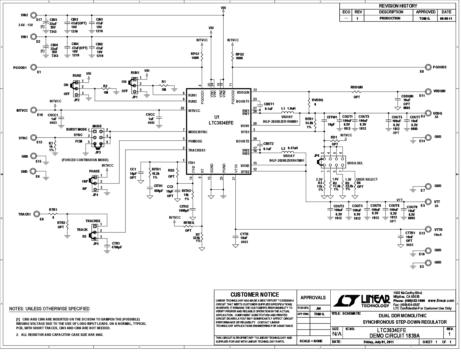
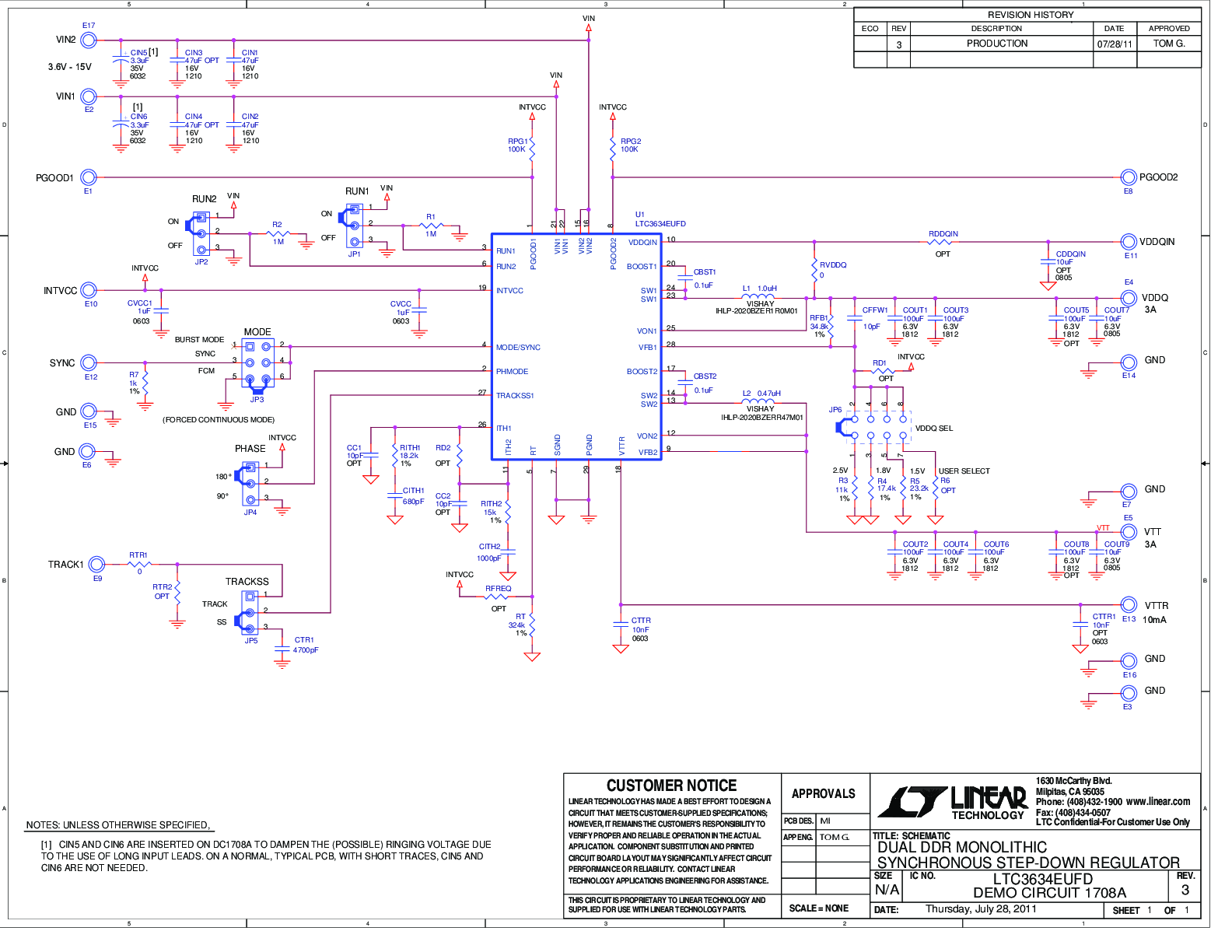
LTC3634
DDRメモリ電源用の15V、デュアル3Aモノリシック降圧レギュレータ
Efficiency and Power Loss vs Load Current Product Package 1 Product Package 2
myAnalogに追加

myAnalogの製品セクション(通知受け取り)、既存/新規プロジェクトに製品を追加する。

新規プロジェクトを作成
質問する
サポート

アナログ・デバイセズのサポート・ページはアナログ・デバイセズへのあらゆるご質問にお答えするワンストップ・ポータルです。


ドキュメント

データシート

これは最新改訂バージョンのデータシートです。

さらに詳しく
myAnalogに追加

myAnalogの製品セクション(通知受け取り)、既存/新規プロジェクトに製品を追加する。

新規プロジェクトを作成

ハードウェア・エコシステム

製品モデル 製品ライフサイクル 詳細
DDR/QDRメモリ/バス終端 1
LTM4632 新規設計に推奨 DDR-QDR4メモリ向けの超薄型トリプル出力降圧µModuleレギュレータ
シリコン発振器 1
LTC6908 スペクトル拡散変調付き抵抗設定SOT-23発振器
デジタル・パワー・システム・マネージメント(PSM) 1
LTC2974 新規設計に推奨 正確な出力電流測定を特長とする4チャンネルPMBusパワーシステム・マネージャ
Modal heading
myAnalogに追加

myAnalogの製品セクション(通知受け取り)、既存/新規プロジェクトに製品を追加する。

新規プロジェクトを作成

ツールおよびシミュレーション

LTspice 1


下記製品はLTspiceで使用することが出来ます。:

  • LTC3634

LTpowerCAD 2

LTspice

LTspice®は、無料で提供される強力で高速な回路シミュレータと回路図入力、波形ビューワに改善を加え、アナログ回路のシミュレーションを容易にするためのモデルを搭載しています。


LTpowerCAD

LTpowerCAD®は、電力段のデバイスの選択、詳細な電力効率の提供、ループのボーデ線図の安定性および負荷過渡応答解析の敏速な表示などを行うと共に、シミュレーション用にLTspiceにエクスポートできる電源設計プログラムです。


評価用キット

eval board
DC1839A

LTC3634EFE Demo Board (TSSOP) | VIN = 3.6V to 15V, VOUT1 = 1.5V/1.8V/2.5V @ ±3A, VOUT2 = 0.5VIN (VTT) @ ±3A, VOUT3 = 0.5VIN (VTTR) @ ±10mA

製品詳細

Demonstration circuit 1839A is a dual output regulator focused specifically for DDR memory power applications. It is built based on the LTC3634EFE (TSSOP-28E package), a high voltage dual channel, controlled on-time monolithic synchronous buck regulator. The DC1839A has an input voltage range of 3.6V to 15V. demo board's output voltage of the first channel, VDDQ, has three fixed voltage settings; 1.5V, 1.8V, and 2.5V, and is capable of delivering up to ±3A of output current. The second channel, VTT, is set to regulate to half the voltage on the VDDQIN pin, which can be either the channel 1 output or an external reference voltage. It can also source or sink a maximum of 3A. The LTC3634 also provides a ±10mA buffered output, VTTR, which is half of VDDQIN and is used to provide the reference voltage needed for DDR applications.

eval board
DC1708A

LTC3634EUFD Demo Board (QFN) | VIN= 3.6V to 15V, VOUT1 =1.5V/1.8V/2.5V@±3A, VOUT2 = 0.5VIN (VTT)@±3A, VOUT3 = 0.5VIN (VTTR)@±10mA

製品詳細

Demonstration circuit DC1708A is a dual-output regulator focused specifically for DDR memory power applications. It is built based on the LTC3634, a high voltage dualchannel, controlled on-time monolithic synchronous buck regulator. The DC1708A has an input voltage range of 3.6V to 15V. The output voltage of the first channel, VDDQ, of the DC1708A has three fixed voltage settings: 1.5V, 1.8V and 2.5V, and is capable of delivering up to 3A of output current. The second channel, VTT, is set to regulate to half the voltage on the VDDQIN pin, which can be either the channel 1 output or an external reference voltage. It can source or sink a maximum of 3A of output current. The LTC3634 also provides a 10mA buffered output of half VDDQIN – VTTR, which is used to provide the reference voltage needed for DDR applications. With the use of a timing resistor, the DC1708A can have its operating frequency programmed from 500kHz to 4MHz. Additionally the DC1708A can be easily synchronized to an external clock, due to an internal phase-locked loop, within this same frequency range. The DC1708A VDDQ output can operate in either Burst Mode® operation or forced continuous mode. In Burst Mode operation, which is the preferred mode of low load current operation, the DC supply current is typically only 1.3mA (both channels) at no load (sleep mode), and less than 15µA in shutdown. In Burst Mode operation or continuous mode operation, the DC1708A is a very efficient circuit at high load currents: over 80% for either channel. The LTC3634 is also capable of 90° or 180° out-of-phase operation, and can allow its output to track an external voltage, either coincidentally or ratiometrically. The LTC3634 comes in a 28-pin QFN package, featuring an exposed pad on the bottom-side of the IC for better thermal performance. All of these features make the DC1708A an ideal circuit for powering DDR memory applications.

DC1839A
LTC3634EFE Demo Board (TSSOP) | VIN = 3.6V to 15V, VOUT1 = 1.5V/1.8V/2.5V @ ±3A, VOUT2 = 0.5VIN (VTT) @ ±3A, VOUT3 = 0.5VIN (VTTR) @ ±10mA
DC1839A - Schematic
DC1708A
LTC3634EUFD Demo Board (QFN) | VIN= 3.6V to 15V, VOUT1 =1.5V/1.8V/2.5V@±3A, VOUT2 = 0.5VIN (VTT)@±3A, VOUT3 = 0.5VIN (VTTR)@±10mA
DC1708A - Schematic

リファレンス・デザイン

Versal AI Core Board
Versal AI Core XCVC1902 Circuits from the Lab®

Edge Core FPGA Power Delivery Reference Design

機能と利点

The ADI Versal AI Core Power Reference Design Board has been tested and proven to power the key rails for the Xilinx Versal AI Core ACAP series. Using a PMBUs Multi Phase DC/DC controller coupled with ADI SilentMOS (ADI version of DrMOS) to deliver up to 240A of output current.

The ADI LTC3888-1 is an 8 Phase PMBUs DC/DC controller that is coupled with the LTC7051 ADI SilentMOS to provide a flexible and scalable design that can be tailored as needed for both higher and lower power applications by adding or subtracting the LTC7051 ADI SilentMOS.

Request schematic for ADI power used on the board.

Contact ADI if you have questions about the ADI power management solutions used on this board.

Versal PRIME Circuits from the Lab®

AI XCXM1802 for Full Management Mid to High Voltage

機能と利点

ADI Key Power Management Features for Versal ACAP XCXM1802 for Mid to High Voltage

  • Proposed Solution implements new LTC3887-1/LTC7051 combo
  • LTC3887-1 is a PMBus 2-phase, 2 loop, current mode controller. PMBus commands allow Vin, Vout, current, temperature, and fault status read back.
  • LTC7051 is new Silent Switcher 2 ADI MOS capable of delivering increased DC load while switching at higher frequencies. Increased DC load allows for decreased phase count and higher current density. Increased Fsw allows for increase bandwidth and excellent transient response.
  • LTC3636 is dual 6A, controlled on-time current mode monolithic (integrated FETs). Provides high performance compact solution for auxiliary rails.
  • LTC3644 is a quad 1.25A output, high efficiency synchronous monolithic capable of switching up to 2.25MHz.
  • LTC3634 is a single chip solution for DDR rails providing VDD, VTT, and Vref in a monolithic solution.
XCXM1802 Low Voltage
Versal PRIME Circuits from the Lab®

AI XCXM1802 for Low Voltage

機能と利点

ADI Key Power Management Features for Versal PRIME XCXM1802 for Low Voltage

  • Proposed Solution implements new LTC3887-1/LTC7051 combo
  • LTC3887-1 is a PMBus 2-phase, 2 loop, current mode controller. PMBus commands allow Vin, Vout, current, temperature, and fault status read back.
  • LTC7051 is new Silent Switcher 2 ADI MOS capable of delivering increased DC load while switching at higher frequencies. Increased DC load allows for decreased phase count and higher current density. Increased Fsw allows for increase bandwidth and excellent transient response.
  • LTC3636 is dual 6A, controlled on-time current mode monolithic (integrated FETs). Provides high performance compact solution for auxiliary rails.
  • LTC3644 is a quad 1.25A output, high efficiency synchronous monolithic capable of switching up to 2.25MHz.
  • LTC3634 is a single chip solution for DDR rails providing VDD, VTT, and Vref in a monolithic solution.
Versal PRIME Circuits from the Lab®

AI XCXM1902 Minimum Rails and PL Performance

機能と利点

ADI Key Power Management Features for Versal PRIME XCXM1802 for Minimum Rails / PL Performance

  • Proposed Solution implements new LTC3887-1/LTC7051 combo
  • LTC3887-1 is a PMBus 2-phase, 2 loop, current mode controller. PMBus commands allow Vin, Vout, current, temperature, and fault status read back.
  • LTC7051 is new Silent Switcher 2 ADI MOS capable of delivering increased DC load while switching at higher frequencies. Increased DC load allows for decreased phase count and higher current density. Increased Fsw allows for increase bandwidth and excellent transient response.
  • LTC3636 is dual 6A, controlled on-time current mode monolithic (integrated FETs). Provides high performance compact solution for auxiliary rails.
  • LT8607 is a compact, high efficiency, high speed 750mA synchronous monolithic.
  • LTC3634 is a single chip solution for DDR rails providing VDD, VTT, and Vref in a monolithic solution.
Versal PRIME Circuits from the Lab®

AI XCXM1802 for Optimized Efficiency

機能と利点

ADI Key Power Management Features for Versal ACAP XCXM1802 for Optimized Efficiency

  • Proposed Solution implements new LTC3887-1/LTC7051 combo
  • LTC3887-1 is a PMBus 2-phase, 2 loop, current mode controller. PMBus commands allow Vin, Vout, current, temperature, and fault status read back.
  • LTC7051 is new Silent Switcher 2 ADI MOS capable of delivering increased DC load while switching at higher frequencies. Increased DC load allows for decreased phase count and higher current density. Increased Fsw allows for increase bandwidth and excellent transient response.
  • LTC3636 is dual 6A, controlled on-time current mode monolithic (integrated FETs). Provides high performance compact solution for auxiliary rails.
  • LTC3634 is a single chip solution for DDR rails providing VDD, VTT, and Vref in a monolithic solution.
  • LTC3634 is a single chip solution for DDR rails providing VDD, VTT, and Vref in a monolithic solution.
Versal AI Core XCVC1902
Edge Core FPGA Power Delivery Reference Design
Versal AI Core Board
Versal AI Core XCVC1902 Power Tree
Versal PRIME
AI XCXM1802 for Full Management Mid to High Voltage
Versal PRIME
AI XCXM1802 for Low Voltage
XCXM1802 Low Voltage
XCXM1802 Low Voltage Efficiency
Versal PRIME
AI XCXM1902 Minimum Rails and PL Performance
Versal PRIME
AI XCXM1802 for Optimized Efficiency

最新のディスカッション

最近表示した製品