ADF4383
ADF4383
新規設計に推奨Microwave Wideband Synthesizer with Integrated VCO
- 製品モデル
- 2
- 1Ku当たりの価格
- 価格は未定
Viewing:
製品の詳細
- Fundamental VCO frequency range: 10 GHz to 20 GHz
- VCO phase noise improvement of up to 3 dB as compared to ADF4382
- Integrated RMS jitter at 20 GHz = 18 fs (integration bandwidth: 100 Hz to 100 MHz)
- Integrated RMS jitter at 20 GHz = 31 fs (ADC SNR method)
- VCO fast calibration time: <2 μs
- VCO autocalibration time: <100 μs
- Phase noise floor: −156 dBc/Hz at 20 GHz
- PLL specifications
- −239 dBc/Hz: normalized in-band phase noise floor (integer mode)
- −287 dBc/Hz: normalized 1/f phase noise floor
- 625 MHz maximum phase/frequency detector input frequency
- 4.5 GHz reference input frequency
- Typical spurious f
PFD: −90 dBc
- Reference to output delay specifications
- Propagation delay temperature coefficient: 0.06 ps/°C
- Adjustment step size: <1 ps
- Multichip output phase alignment
- 3.3 V and 5 V power supplies
- ADIsimPLL™ loop filter design tool support
- 7 mm × 7 mm, 48-terminal LGA
- −40°C to +105°C operating temperature
The ADF4383 is a high performance, ultra-low jitter, fractional-N phased-locked loop (PLL) with an integrated voltage controlled oscillator (VCO) ideally suited for local oscillator (LO) generation for 5G applications or data converter clock applications. The high performance PLL has a figure of merit of −239 dBc/Hz, low 1/f noise and high PFD frequency of 625 MHz in integer mode that can achieve ultra-low in-band noise and integrated jitter. The ADF4383 can generate frequencies in a fundamental octave range of 10 GHz to 20 GHz, thereby eliminating the need for subharmonic filters. The output dividers on the ADF4383 allows a complete output frequency range to be generated from 625 MHz to 20 GHz.
For multiple data converter clock applications, the ADF4383 automatically aligns its output to the input reference edge by including the output divider in the PLL feedback loop. For applications that require deterministic delay or delay adjustment capability, a programmable reference to output delay with <1 ps resolution is provided. The reference to output delay matching across multiple devices and over temperature allows predictable and precise multichip alignment.
The simplicity of the ADF4383 block diagram eases development time with a simplified serial peripheral interface (SPI) register map, external SYNC input, and repeatable multichip alignment in both integer and fractional mode.
APPLICATIONS
- High performance data converter clocking
- Wireless infrastructure (MC-GSM, 5G, 6G)
- Test and measurement
ドキュメント
| 製品モデル | ピン/パッケージ図 | 資料 | CADシンボル、フットプリント、および3Dモデル |
|---|---|---|---|
| ADF4383BCCZ | LGA/CASON/CH ARRY SO NO LD | ||
| ADF4383BCCZ-RL7 | LGA/CASON/CH ARRY SO NO LD |
これは最新改訂バージョンのデータシートです。
ハードウェア・エコシステム
| 製品モデル | 製品ライフサイクル | 詳細 |
|---|---|---|
| LDOプラス 1 | ||
| LT3042 | 新規設計に推奨 | 20V、200mA、超低ノイズ、超高PSRRのRFリニア・レギュレータ |
| クロック生成デバイス 1 | ||
| HMC7044B | 新規設計に推奨 | JESD204BおよびJESD204Cをサポートする高性能、3.2GHz、14出力ジッタ減衰器 |
| クロック同期 1 | ||
| ADF4030 | 新規設計に推奨 | 10チャンネル高精度シンクロナイザ |
| ミックスド・シグナル・フロントエンド(MxFE) 1 | ||
| AD9084 | 発売前 | Apollo MxFE、16ビット28GSPSクワッドRF DACおよび12ビット20GSPSクワッドRF ADC |
| 高速コンパレータ(伝播遅延100ns未満) 1 | ||
| LTC6957 | 位相ノイズの小さいデュアル出力バッファ/ドライバ/ロジック・コンバータ | |
| 正電圧のリニア電圧レギュレータ(LDO) 2 | ||
| LT3041 | 新規設計に推奨 | 20V、1A、超低ノイズ、超高PSRRのVIOC制御搭載リニア電圧レギュレータ |
| LT3045 | 新規設計に推奨 | 20V、500mA、超低ノイズ、超高PSRRのリニア・レギュレータ |
ツールおよびシミュレーション
ADIsimPLL™
ADIsimPLLは、アナログ・デバイセズの新しい高性能PLL製品の迅速で信頼性の高い評価を可能にします。これは、現在利用できる最も包括的なPLLシンセサイザ設計およびシミュレーション・ツールです。実施されるシミュレーションには、PLL性能に影響を与える重要な非線形効果がすべて含まれます。ADIsimPLLは、設計プロセスから1回以上の反復作業を削除し、設計から市場投入までの時間を短縮します。
ツールを開くIBISモデル 1
評価用キット
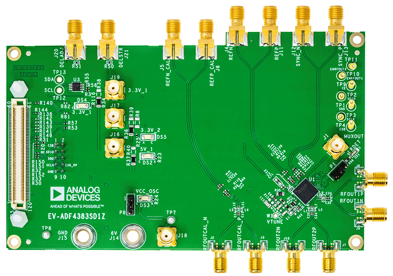
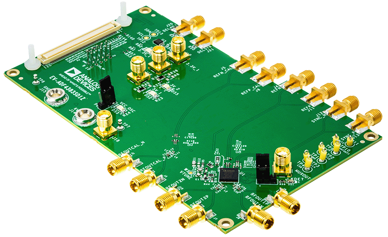
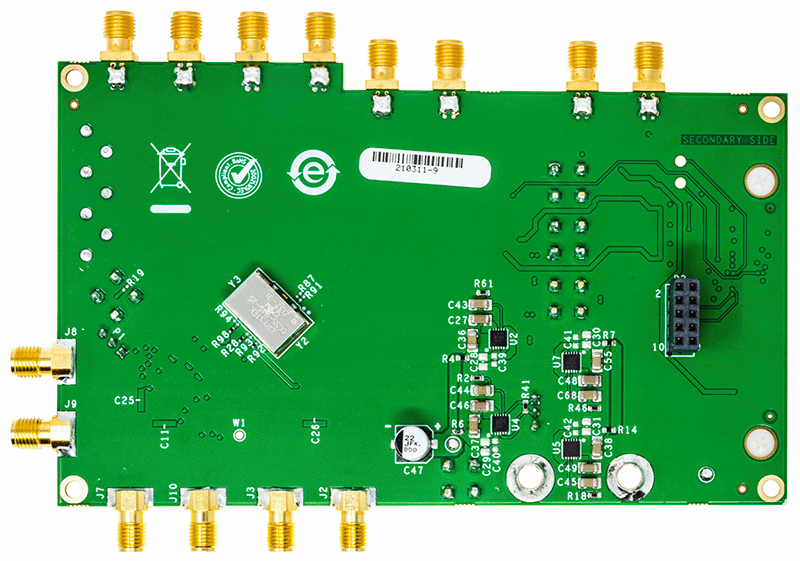
Evaluating the ADF4383 Microwave Wideband Synthesizer with Integrated VCO
資料
ソフトウェア
最新のディスカッション
adf4383に関するディスカッションはまだありません。意見を投稿しますか?
EngineerZone®でディスカッションを始める