ADF4383
推荐新设计使用集成 VCO 的微波宽带频率合成器
- 产品模型
- 2
产品详情
- 基本 VCO 频率范围:10 GHz 至 20 GHz
- 与 ADF4382 相比,VCO 相位噪声改善高达 3 dB
- 20 GHz 时的积分 RMS 抖动 = 18 fs(积分带宽:100 Hz 至 100 MHz)
- 20 GHz 时的积分 RMS 抖动 = 31 fs(ADC SNR 方法)
- VCO 快速校准时间:<2 μs
- VCO 自动校准时间:<100 μs
- 相位本底噪声:20 GHz 时为 −156 dBc/Hz
- PLL 规格
- −239dBc/Hz:归一化带内相位噪声基底(整数模式)
- −287dBc/Hz:归一化 1/f 相位本底噪声
- 625 MHz 最大相位/频率检波器输入频率
- 4.5 GHz 参考输入频率
- 典型杂散 f
PFD:−90 dBc
- 参考输出延迟规格
- 传播延迟温度系数:0.06 ps/°C
- 调整步长:<1ps
- 多芯片输出相位对齐
- 3.3V 和 5V 电源
- 支持 ADIsimPLL™ 环路滤波器设计工具
- 7 mm × 7 mm、48 端子 LGA
- 工作温度 −40°C 至 +105°C
ADF4383 是一款高性能、超低抖动、小数 N 分频锁相环 (PLL),带有集成电压控制振荡器 (VCO),非常适合 5G 应用或数据转换器时钟应用的本地振荡器 (LO) 生成。高性能 PLL 具有 −239 dBc/Hz 的品质因数、低 1/f 噪声和整数模式下 625 MHz 的高 PFD 频率,可实现超低带内噪声和综合抖动。ADF4383 可产生 10 GHz 至 20 GHz 基本倍频范围内的频率,从而无需使用次谐波滤波器。ADF4383 上的输出分频器可产生从 625 MHz 至 20 GHz 的完整输出频率范围。
对于多数据转换器时钟应用,ADF4383 通过在 PLL 反馈环路中包含输出分频器,自动将其输出与输入参考边沿对齐。对于需要确定性延迟或延迟调整功能的应用,提供分辨率 <1 ps 的可编程输出延迟参考。通过参考跨多个设备和整个温度的输出延迟匹配,可以实现可预测且精确的多芯片对齐。
ADF4383 框图十分简单,通过简化的串行外设接口 (SPI) 寄存器映射、外部 SYNC 输入以及整数和小数模式下可重复的多芯片对齐,可以缩短开发时间。
应用
- 高性能数据转换器时钟
- 无线基础设施(MC-GSM、5G、6G)
- 测试和测量
参考资料
ADI 始终高度重视提供符合最高质量和可靠性水平的产品。我们通过将质量和可靠性检查纳入产品和工艺设计的各个范围以及制造过程来实现这一目标。出货产品的“零缺陷”始终是我们的目标。查看我们的质量和可靠性计划和认证以了解更多信息。
| 产品型号 | 引脚/封装图-中文版 | 文档 | CAD 符号,脚注和 3D模型 |
|---|---|---|---|
| ADF4383BCCZ | LGA/CASON/CH ARRY SO NO LD | ||
| ADF4383BCCZ-RL7 | LGA/CASON/CH ARRY SO NO LD |
这是最新版本的数据手册
软件资源
找不到您所需的软件或驱动?
申请驱动/软件硬件生态系统
| 部分模型 | 产品周期 | 描述 |
|---|---|---|
| LDO+ 1 | ||
| LT3042 | 推荐新设计使用 | 20V、200mA、超低噪声、超高 PSRR RF 线性稳压器 |
| 高速比较器(传播延迟<100ns) 1 | ||
| LTC6957 | 低相位噪声、双输出缓冲器 / 驱动器 / 逻辑转换器 | |
| 混合信号前端(MxFE) 1 | ||
| AD9084 | 预发布 | Apollo MxFE Quad, 16-Bit, 28 GSPS RF DAC and Quad, 12-Bit, 20 GSPS RF ADC |
| 时钟产生器件 1 | ||
| HMC7044B | 推荐新设计使用 | 支持 JESD204B 和 JESD204C 的高性能、3.2 GHz、14 输出抖动衰减器 |
| 时钟同步 1 | ||
| ADF4030 | 推荐新设计使用 | 10-Channel Precision Synchronizer |
| 正线性稳压器(LDO) 2 | ||
| LT3041 | 推荐新设计使用 | 具有 VIOC 的 20 V、1 A、超低噪声、超高 PSRR 线性稳压器 |
| LT3045 | 推荐新设计使用 | 20V、500mA、超低噪声、超高 PSRR 线性稳压器 |
工具及仿真模型
IBIS 模型 1
ADIsimPLL™
ADIsimPLL可以对ADI公司最新的高性能PLL产品进行快速、可靠的评估。它是目前最全面的PLL频率合成器设计和仿真工具,可实现所有对PLL性能有显著影响的重要非线性效应仿真。ADIsimPLL可以免去设计过程中的至少一项重复劳动,从而加快上市速度。
打开工具评估套件
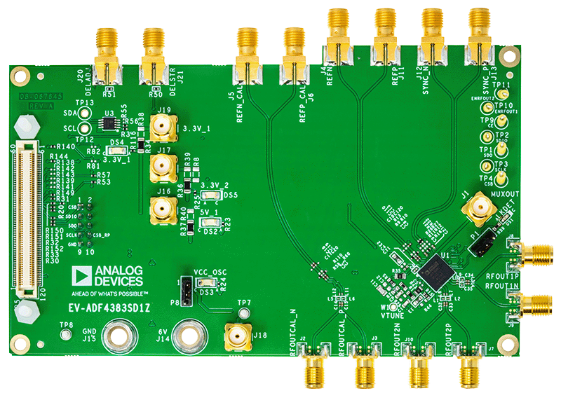
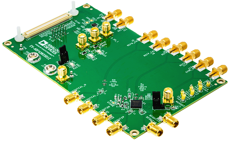
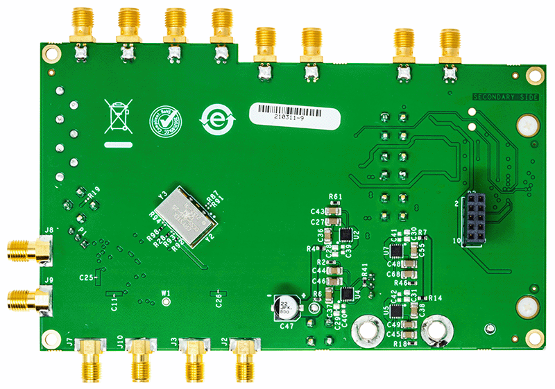
评估带集成 VCO 的 ADF4383 微波宽带频率合成器
资料
软件
最新评论
需要发起讨论吗? 没有关于 ADF4383的相关讨论?是否需要发起讨论?
在EngineerZone®上发起讨论