LTC3308A
新規設計に推奨5V、4A同期整流降圧Silent Switcher(2mm × 2mm LQFN)
- 製品モデル
- 18
- 1Ku当たりの価格
- 最低価格:$2.18
製品の詳細
- LTC3307(3A)およびLTC3309(6A)とピン互換
- 高効率:8mΩ NMOS、31mΩ PMOS
- プログラマブルな周波数:1MHz~3MHz
- 小型のインダクタとキャパシタ
- ピーク電流モード制御
- 22ns最小オン時間
- 広帯域幅、高速過渡応答
- Silent Switcher™アーキテクチャ
- 超低EMI放射
- 40μA IQの低リップル バースト・モード®動作
- 過負荷におけるインダクタの飽和状態に対する安全な耐性
- VIN 範囲:2.25V~5.5V
- VOUT範囲:0.5V~VIN
- VOUT精度:±1%の温度範囲
- 高精度400mVイネーブル閾値、シャットダウン時電流1μA
- パワーグッド、内部補償機能とソフトスタート機能
- 熱強化型2mm × 2mm LQFNパッケージ
- オートモーティブ・アプリケーション向けのAEC-Q100認定済み
LTC3308Aは非常に小さく、高効率かつ低ノイズのモノリシック同期整流式4A降圧DC/DCコンバータです。2.25V~5.5Vの入力電源で動作します。固定周波数、1MHz~3MHzのスイッチング周波数でのピーク電流モード制御、わずか22nsの最小オン時間を特長とするこのレギュレータは、わずかな外付け部品で高速の過渡応答を実現します。Silent SwitcherアーキテクチャによってEMI放射が最小限に抑えられます。
LTC3308Aは、低ノイズの強制連続モードまたはパルス・スキップ・モード、または軽負荷で高効率の低リップルのバースト・モードで動作するため、バッテリ駆動システムに最適です。ICは、出力電圧をわずか500mVほどの低圧に調整できます。更に、出力の過電圧保護/短絡保護、サーマル・シャットダウン、クロック同期、100%デューティ・サイクルまでの低ドロップアウト動作の各機能を搭載しています。このデバイスは、熱抵抗を低く抑えるための露出パッドが付いた、薄型の12ピン2mm × 2mm × 0.74mm LQFNパッケージを採用しています。
アプリケーション
- 光ネットワーク、サーバー、テレコム
- オートモーティブ、産業、通信
- 分散型DC電源システム(POL)
- FPGA、ASIC、μPコア電源
- バッテリ駆動システム
ドキュメント
データシート 2
信頼性データ 1
Book & eBook 1
ソリューション・カタログ 1
Analog Dialogue 1
珍問/難問集 1
| 製品モデル | ピン/パッケージ図 | 資料 | CADシンボル、フットプリント、および3Dモデル |
|---|---|---|---|
| LTC3308AEV#TRMPBF | 12-Lead LQFN (2mm x 2mm x 0.74mm) | ||
| LTC3308AEV#TRPBF | 12-Lead LQFN (2mm x 2mm x 0.74mm) | ||
| LTC3308AEV#WTRMPBF | 12-Lead LQFN (2mm x 2mm x 0.74mm) | ||
| LTC3308AEV#WTRPBF | 12-Lead LQFN (2mm x 2mm x 0.74mm) | ||
| LTC3308AHV#TRMPBF | 12-Lead LQFN (2mm x 2mm x 0.74mm) | ||
| LTC3308AHV#TRPBF | 12-Lead LQFN (2mm x 2mm x 0.74mm) | ||
| LTC3308AHV#WTRMPBF | 12-Lead LQFN (2mm x 2mm x 0.74mm) | ||
| LTC3308AHV#WTRPBF | 12-Lead LQFN (2mm x 2mm x 0.74mm) | ||
| LTC3308AIV#TRMPBF | 12-Lead LQFN (2mm x 2mm x 0.74mm) | ||
| LTC3308AIV#TRPBF | 12-Lead LQFN (2mm x 2mm x 0.74mm) | ||
| LTC3308AIV#WTRMPBF | 12-Lead LQFN (2mm x 2mm x 0.74mm) | ||
| LTC3308AIV#WTRPBF | 12-Lead LQFN (2mm x 2mm x 0.74mm) | ||
| LTC3308AJV#TRMPBF | 12-Lead LQFN (2mm x 2mm x 0.74mm) | ||
| LTC3308AJV#TRPBF | 12-Lead LQFN (2mm x 2mm x 0.74mm) | ||
| LTC3308AJV#WTRMPBF | 12-Lead LQFN (2mm x 2mm x 0.74mm) | ||
| LTC3308AJV#WTRPBF | 12-Lead LQFN (2mm x 2mm x 0.74mm) | ||
| LTC3308AMPV#TRMPBF | 12-Lead LQFN (2mm x 2mm x 0.74mm) | ||
| LTC3308AMPV#TRPBF | 12-Lead LQFN (2mm x 2mm x 0.74mm) |
これは最新改訂バージョンのデータシートです。
ソフトウェア・リソース
必要なソフトウェア/ドライバが見つかりませんか?
ドライバ/ソフトウェアをリクエストツールおよびシミュレーション
LTspice
下記製品はLTspiceで使用することが出来ます。:
- LTC3308A
- LTC3308B
LTpowerCAD 1
次のデバイス用の設計ツールがLTpowerCADでご使用になれます。
- LTC3308A
- LTC3308B
LTspice®は、無料で提供される強力で高速な回路シミュレータと回路図入力、波形ビューワに改善を加え、アナログ回路のシミュレーションを容易にするためのモデルを搭載しています。
LTpowerCAD®は、電力段のデバイスの選択、詳細な電力効率の提供、ループのボーデ線図の安定性および負荷過渡応答解析の敏速な表示などを行うと共に、シミュレーション用にLTspiceにエクスポートできる電源設計プログラムです。
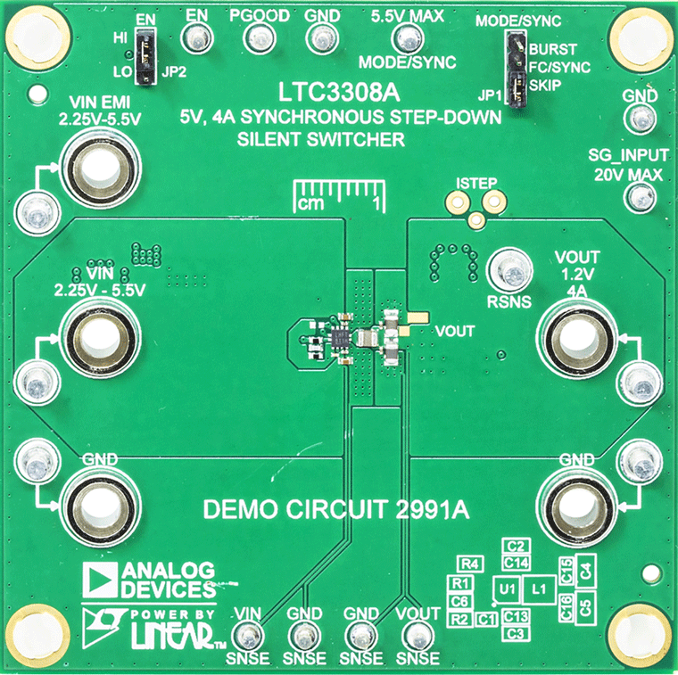
評価用キット
LTC3308A Demo Board | 5V Input to 1.2V Output at 4A Synchronous Step‑Down Silent Switcher Demo Circuit