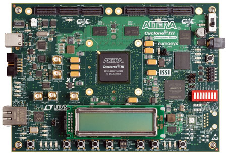
LTC3203

製造中

500mA出力電流、低ノイズ、デュアルモード昇圧チャージポンプ

製品モデル
8
1Ku当たりの価格
最低価格:$2.67
利用上の注意

アナログ・デバイセズ社は、提供する情報が正確で信頼できるものであることを期していますが、その情報の利用に関して、あるいはその利用によって生じる第三者の特許やその他の権利の侵害に関して一切の責任を負いません。また、アナログ・デバイセズ社の特許または特許の権利の使用を明示的または暗示的に許諾するものでもありません。仕様は予告なしに変更する場合があります。本紙記載の商標および登録商標は、各社の所有に属します。


本データシートの英語以外の言語への翻訳はユーザの便宜のために提供されるものであり、リビジョンが古い場合があります。最新の内容については、必ず最新の英語版をご参照ください。

なお、日本語版のデータシートは基本的に「Rev.0」(リビジョン0)で作成されています。そのため、英語版が後に改訂され、複数製品のデータシートがひとつに統一された場合、同じ「Rev.0」の日本語版のデータシートが異なる製品のデータシートとして表示されることがあります。たとえば、「ADM3307E」の場合、日本語データシートをクリックすると「ADM3311E」が表示されます。これは、英語版のデータシートが複数の製品で共有できるように1本化され、「ADM3307E/ADM3310E/ADM3311E/ADM3312E/ADM3315E」(Rev.G)と改訂されたからで、決して誤ってリンクが張られているわけではありません。和文化されたデータシートを少しでも有効に活用していただくためにこのような方法をとっておりますので、ご了解ください。

Viewing:

製品の詳細

  • 選択可能なデュアルモード動作:1:1.5または1:2
  • 高出力電流:最大500mA
  • 低ノイズ固定周波数(1MHz/0.9MHz)動作
  • VIN 範囲:2.7V ~ 5.5V
  • 可変出力電圧(LTC3203/LTC3203B)
  • ユーザが選択可能な固定出力電圧:4.5Vまたは5V(LTC3203-1またはLTC3203B-1)
  • 消費電流が120μAの自動Burst Mode®動作(LTC3203/LTC3203-1)
  • 全負荷での固定周波数動作(LTC3203B/LTC3203B-1)
  • ソフトスタートにより、起動時の突入電流を制限
  • 短絡/熱保護機能
  • シャットダウン時に入力から負荷を切断
  • シャットダウン電流:<1μA
  • 10ピン3mm×3mm DFNパッケージで供給
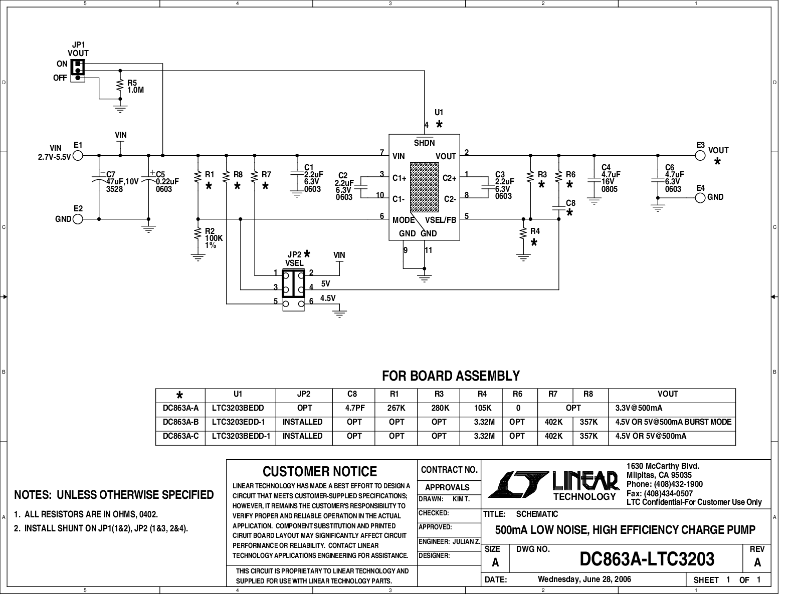
LTC3203
500mA出力電流、低ノイズ、デュアルモード昇圧チャージポンプ
Efficiency vs VIN at 300mA Load Current Product Package 1
myAnalogに追加

myAnalogの製品セクション(通知受け取り)、既存/新規プロジェクトに製品を追加する。

新規プロジェクトを作成
質問する
サポート

アナログ・デバイセズのサポート・ページはアナログ・デバイセズへのあらゆるご質問にお答えするワンストップ・ポータルです。


ドキュメント

データシート

これは最新改訂バージョンのデータシートです。

さらに詳しく
myAnalogに追加

myAnalogの製品セクション(通知受け取り)、既存/新規プロジェクトに製品を追加する。

新規プロジェクトを作成

ツールおよびシミュレーション

LTspice

LTspice®は、無料で提供される強力で高速な回路シミュレータと回路図入力、波形ビューワに改善を加え、アナログ回路のシミュレーションを容易にするためのモデルを搭載しています。


評価用キット

eval board
DC863A-C

LTC3203B-1 Demo Board | Regulated Boost Charge Pump, 2.7V ≤ VIN ≤ 5.5V, VOUT = 4.5V or 5V @ Up to 500mA

製品詳細

Demonstration circuit 863 is a high efficiency regulated boost charge pump converter that exercises the 500mA low noise LTC3203 in the 3mm x 3mm DFN package. It comes with three assembly versions, DC863A-A (3.3V output), DC863A-B (4.5V or 5V output) and DC863A-C (4.5V or 5V output), featuring the LTC3203B, LTC3203-1, and LTC3203B-1 respectively. The input voltage range is from 2.7V to 5.5V. The output current can reach up to 500mA with an input voltage above 2.9V for a 4.5V output, above 3.1V for a 5V output and over the full input range for a 3.3V output. By choosing the proper operation modes, the DC863A circuit optimizes conversion efficiencies and maintains the maximum output current at each output voltage.


Additionally, DC863A-B features Automatic Burst Mode operation at light load to achieve low supply current, whereas DC863A-A and DC863A-C operate in constant frequency mode to achieve low noise at the input. The built-in soft-start prevents excessive inrush current at start-up, and short-circuit current limit/thermal protection help the part survive a continuous short-circuit.

eval board
DC863A-B

LTC3203-1 Demo Board | Regulated Boost Charge Pump, 2.7V ≤ VIN ≤ 5.5V, VOUT = 4.5V or 5V @ Up to 500mA

製品詳細

Demonstration circuit 863 is a high efficiency regulated boost charge pump converter that exercises the 500mA low noise LTC3203 in the 3mm x 3mm DFN package. It comes with three assembly versions, DC863A-A (3.3V output), DC863A-B (4.5V or 5V output) and DC863A-C (4.5V or 5V output), featuring the LTC3203B, LTC3203-1, and LTC3203B-1 respectively. The input voltage range is from 2.7V to 5.5V. The output current can reach up to 500mA with an input voltage above 2.9V for a 4.5V output, above 3.1V for a 5V output and over the full input range for a 3.3V output. By choosing the proper operation modes, the DC863A circuit optimizes conversion efficiencies and maintains the maximum output current at each output voltage.


Additionally, DC863A-B features Automatic Burst Mode operation at light load to achieve low supply current, whereas DC863A-A and DC863A-C operate in constant frequency mode to achieve low noise at the input. The built-in soft-start prevents excessive inrush current at start-up, and short-circuit current limit/thermal protection help the part survive a continuous short-circuit.

eval board
DC863A-A

LTC3203B Demo Board | Regulated Boost Charge Pump, 2.7V ≤ VIN ≤ 4V, VOUT = 3.3V @ Up to 500mA

製品詳細

Demonstration circuit 863 is a high efficiency regulated boost charge pump converter that exercises the 500mA low noise LTC3203 in the 3mm x 3mm DFN package. It comes with three assembly versions, DC863A-A (3.3V output), DC863A-B (4.5V or 5V output) and DC863A-C (4.5V or 5V output), featuring the LTC3203B, LTC3203-1, and LTC3203B-1 respectively. The input voltage range is from 2.7V to 5.5V. The output current can reach up to 500mA with an input voltage above 2.9V for a 4.5V output, above 3.1V for a 5V output and over the full input range for a 3.3V output. By choosing the proper operation modes, the DC863A circuit optimizes conversion efficiencies and maintains the maximum output current at each output voltage.


Additionally, DC863A-B features Automatic Burst Mode operation at light load to achieve low supply current, whereas DC863A-A and DC863A-C operate in constant frequency mode to achieve low noise at the input. The built-in soft-start prevents excessive inrush current at start-up, and short-circuit current limit/thermal protection help the part survive a continuous short-circuit.

DC863A-C
LTC3203B-1 Demo Board | Regulated Boost Charge Pump, 2.7V ≤ VIN ≤ 5.5V, VOUT = 4.5V or 5V @ Up to 500mA
DC863A-A - Schematic
DC863A-B
LTC3203-1 Demo Board | Regulated Boost Charge Pump, 2.7V ≤ VIN ≤ 5.5V, VOUT = 4.5V or 5V @ Up to 500mA
DC863A-A - Schematic
DC863A-A
LTC3203B Demo Board | Regulated Boost Charge Pump, 2.7V ≤ VIN ≤ 4V, VOUT = 3.3V @ Up to 500mA
DC863A-A - Schematic

リファレンス・デザイン

DK-DEV-3CLS200N Dev Kit
Altera Cyclone III LS FPGA Development Kit Circuits from the Lab®

機能と利点

  • Analog Devices has worked closely with FPGA and processor manufacturers to develop verified power solutions that optimize cost, size and efficiency in high performance applications
  • Our reference designs are supported by an intuitive design tool set and IP
  • Our team can provide designs for quick prototypes that can speed time to market in the most complex applications
Altera Cyclone III LS FPGA Development Kit
DK-DEV-3CLS200N Dev Kit
LTC Parts List
DK-DEV-3CLS200N Block Diagram
Cyclone III LS FPGA Development Kit

最新のディスカッション

最近表示した製品