ADL8102
新規設計に推奨GaAs、pHEMT、MMIC、低ノイズ・アンプ、1GHz~22GHz
- 製品モデル
- 2
- 1Ku当たりの価格
- 最低価格:$95.67
製品の詳細
- 正側(供給)単電源(自己バイアス)
- ゲイン:9GHz~19GHzで27dB(代表値)
- OP1dB:1GHz~9GHzで13.5dB(代表値)
- OIP3:1GHz~9GHzで25dBm(代表値)
- ノイズ指数:9GHz~19GHzで2.5dB(代表値)
- RoHS準拠、3mm × 3mm、16ピン、LFCSPパッケージ
ADL8102は、ガリウム・ヒ素(GaAs)、モノリシック・マイクロ波集積回路(MMIC)、擬似格子整合型高電子移動度トランジスタ(pHEMT)、低ノイズ広帯域アンプで、動作範囲は1GHz~22GHzです。
ADL8102は、9GHz~19GHzの範囲で27dB(代表値)のゲイン、9GHz~19GHzの範囲で2.5dB(代表値)のノイズ指数、1GHz~9GHzの範囲で25dBm(代表値)の出力3次インターセプト・ポイント(OIP3)、最大15.5dBmの飽和出力電力(PSAT)を達成するほか、5V電源から要するのはわずか110mAです。また、ADL8102の入出力は内部で50Ωに整合されています。RFINおよびRFOUTピンは内部でACカップリングされ、バイアス・インダクタも内蔵されているため、表面実装技術(SMT)ベースの大容量マイクロ波無線アプリケーションに最適です。
ADL8102は、RoHS準拠の3mm × 3mm、16ピンLFCSPパッケージに収められています。
アプリケーション
ドキュメント
データシート 2
ユーザ・ガイド 1
アプリケーション・ノート 2
| 製品モデル | ピン/パッケージ図 | 資料 | CADシンボル、フットプリント、および3Dモデル |
|---|---|---|---|
| ADL8102ACPZN | 16-Lead LFCSP (3mm x 3mm w/ EP) | ||
| ADL8102ACPZN-R7 | 16-Lead LFCSP (3mm x 3mm w/ EP) |
| 製品モデル | 製品ライフサイクル | PCN |
|---|---|---|
|
9 28, 2023 - 23_0146 Process Revision for Select Low Noise Amplifier Products |
||
| ADL8102ACPZN | 製造中 | |
| ADL8102ACPZN-R7 | 製造中 | |
これは最新改訂バージョンのデータシートです。
ソフトウェア・リソース
必要なソフトウェア/ドライバが見つかりませんか?
ドライバ/ソフトウェアをリクエストツールおよびシミュレーション
Sパラメータ 1
評価用キット
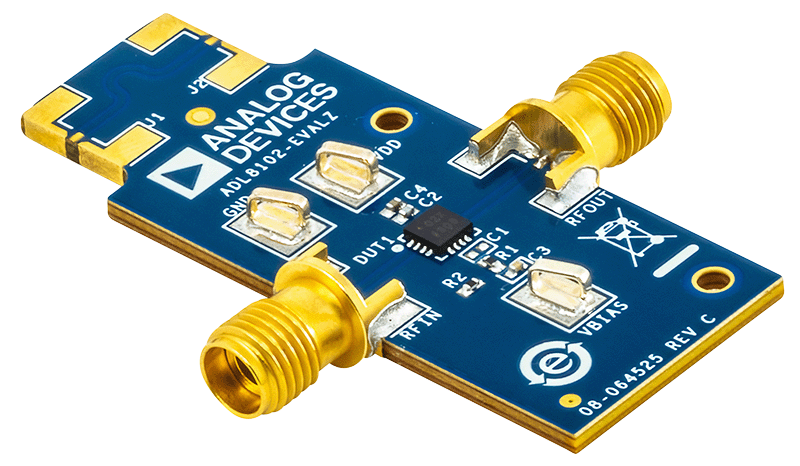
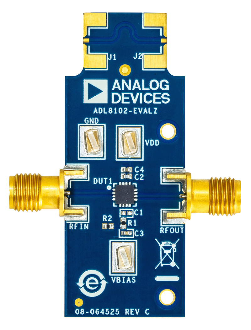
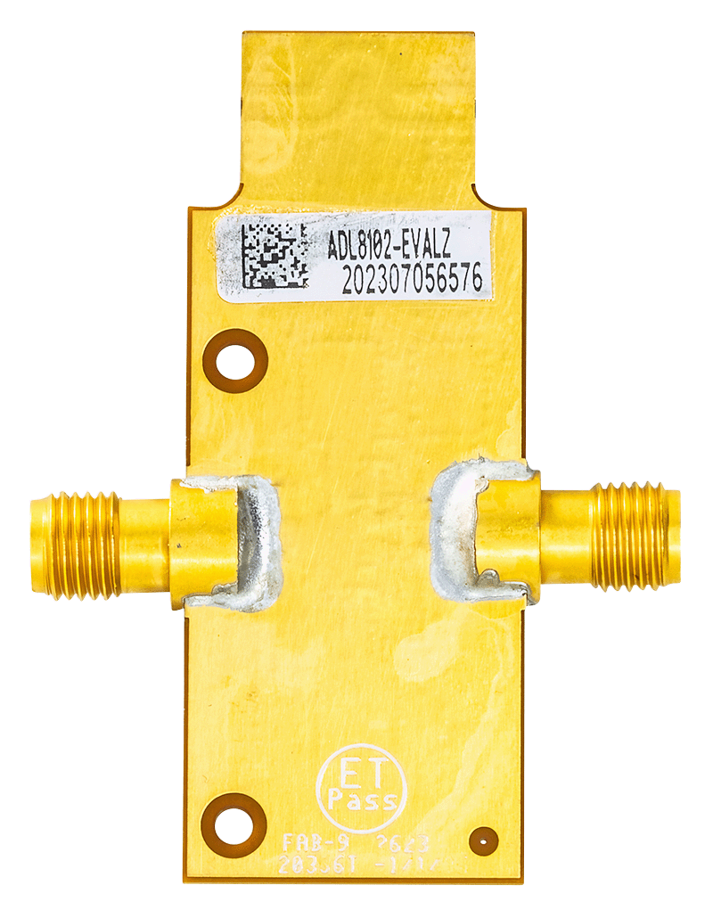
Evaluating the ADL8102 Wideband, Low Noise Amplifier, Single Positive Supply, 1 GHz to 20 GHz
資料
最新のディスカッション
ADL8102に関するディスカッションはまだありません。意見を投稿しますか?
EngineerZone®でディスカッションを始める