CN0314


Overview
Design Resources
Design & Integration File
- Schematic
- Bill of Materials
- Gerber Files
- Allegro Layout Files
- Assembly Drawing
Evaluation Hardware
Part Numbers with "Z" indicate RoHS Compliance. Boards checked are needed to evaluate this circuit.
- EVAL-CN0314-EB1Z ($76.51) Configurable 4-20 mA Loop Powered Transmitter/Receiver using a Micropower Instrumentation Amplifier
Features & Benefits
- 4-20mA Transmitter/Receiver
- Loop Powered
- Configurable
Product Categories
Markets and Technologies
Parts Used
Documentation & Resources
-
MT-066: In-Amp Bridge Circuit Error Budget Analysis2/14/2015PDF35 kB
-
MT-035: Op Amp Inputs, Outputs, Single-Supply, and Rail-to-Rail Issues2/14/2015PDF115 kB
-
MT-031: Grounding Data Converters and Solving the Mystery of "AGND" and "DGND"3/20/2009PDF144 kB
Circuit Function & Benefits
The circuit shown in Figure 1 is a configurable 4 mA-to-20 mA loop-powered transmitter based on an industry-leading micropower instrumentation amplifier. Total unadjusted error is less than 1%. It can be configured with a single switch as either a transmitter (Figure 1) that converts a differential input voltage into a current output, or as a receiver (Figure 5) that converts a 4 mA-to-20 mA current input to a voltage output.


The design is optimized for precision, low noise and low power industrial process control applications. The circuit can accept 0 V to 5V or 0 V to 10 V input range as a transmitter. As a receiver it can provide 0.2 V to 2.3 V or 0.2 V to 4.8 V output range compatible with ADCs using 2.5 V or 5 V references. The supply voltage can range from 12 V to 36 V as a transmitter and 7 V to 36 V as a receiver.
Since the circuit is configurable, a single hardware design can be used as a backup for both transmitter and receiver at the same time, minimizing customer inventory requirements.
Circuit Description
The circuit features the AD8420, an instrumentation amplifier based on an indirect current feedback architecture. Because of this architecture, the AD8420 has excellent input and output characteristics. Unlike conventional instrumentation amplifiers, the AD8420 can easily amplify signals at or even slightly below ground without requiring dual supplies. The AD8420 has rail-to-rail output voltage swing that is completely independent of the input common-mode voltage. This exempts the AD8420 from the restrictions caused by interaction between the common-mode input and output voltage associated with most conventional instrumentation amplifier architectures. The flexible input and output characteristics, together with micropower consumption (80 μA maximum for 0 V input) and wide supply range, make the AD8420 ideal for flexible low power industrial applications.
Transmitter Configuration
Figure 1 shows the simplified schematic for the 4mA-to-20mA transmitter configuration. The circuit only consumes around 1 mA of current, which makes it suitable for loop-powered applications. The transmitter has input ranges of 0 V to 5 V and 0 V to 10 V, which can be selected using the jumper link P3. The input voltage range is then scaled down to 0.195 V to 0.990 V range since the differential input voltage of AD8420 is limited to maximum of 1 V.
The input to the AD8420 has a differential mode noise filter (40 kΩ/3.3 nF) with a 1.2 kHz bandwidth and a common-mode noise filter (20 kΩ/330 pF) with a 24 kHz bandwidth.
The indirect current feedback architecture of AD8420 forces the differential input voltage of the amplifier to appear between its FB and REF pins. The transistor Q1 then translates the 0.195 V to 0.990 V range into 3.9 mA to 19.8 mA flowing through the R9 50 Ω sense resistor.
The current through the R9 sense resistor includes the circuit current and the Q1 current, but not the AD8420 current, IAMP.
The unique architecture of the AD8420 makes its supply current redictable from 100 μA to 200 μA for a 0.195 V to 0.990 V input applied between +IN and −IN. This supply current will add to the current through R9, bringing the total output loop current to 4 mA-to-20 mA. Therefore, the total current in the loop is given by the equation:

In order for the circuit to operate properly, the total circuit supply voltage must be greater than 7 V to provide sufficient headroom for the ADR02 voltage reference.

The loop supply voltage is also limited to 36 V maximum. An advantage of AD8420 is its high impedance reference pin that eliminates the need for an additional op-amp to drive it, thus, saving power, cost and space in the transmitter circuit. It is important for proper loop operation that the circuit board ground and the loop ground are not connected except for the R9, 50 Ω sense resistor.
Selection of Scaling Resistors
The differential input voltage range of AD8420 is limited to maximum of ±1V. Hence, to be able to accept higher industrial input voltage range, the circuit makes use of a scaling resistor network to translate the 0 V to 5 V or 0 V to 10 V input into 0.195 V to 0.990 V. The following equations use nodal analysis to obtain the values for R1, R2, R3, and R4 in the circuit:

Again, solving for the corresponding scaling resistors:

In the practical circuit, the nearest EIA standard 0.1% resistor values must be chosen, resulting in fixed offset error. The resistors supplied with the EVAL-CN0314-EB1Z board are as follows:

With these values supplied with the board, the offset errors due to the resistor values can be computed using the following equations:
For 0 V to 5 V inputs; VREF = 5 V; R1 = 5.05 kΩ; R2 = 20.5 kΩ and R5 = 1 kΩ.

To minimize this offset error, it is also possible to use combination of two 0.1% values to come closer to the calculated resistor values.
Total Transmitter Circuit Accuracy
A good approximation of the total error contributed by the resistor tolerances is to assume that each of the critical resistors contributes equally to the total error. The four critical resistors are R1 or R3, R2 or R4, R5 and R9. Worst-case tolerance build up of 0.1% resistors yield a total resistor error of 0.4% maximum. If rss errors are assumed, the total rss error is 0.1√4 = 0.2%.
The maximum and rss errors due to the active components in the system using the A grade for AD8420 and B grade for levels of ADR02 are shown in the table below.
| Error Component | Error | Error Value | Error %FSR |
| AD8420-A | Offset | 250 µV | 0.03% |
| ADR02-B | Offset | 0.06% | 0.015% |
| RSS FS Error | 0.034% | ||
| Max FS Error | 0.045% |
Adding the worst case resistor tolerance error of 0.4% to the worst-case errors due to the offsets of active components yields:

These errors assume that ideal resistors were selected and the errors resulted from their tolerances.
Actual error data from the circuit is shown in Figure 3 and Figure 4 with a loop supply = 25 V. The total output error (%FSR) is calculated by taking the difference between the measured output current and the ideal output current, dividing by the FSR (16 mA), and multiplying the result by 100.


Receiver Configuration
The simplified receiver configuration is illustrated in Figure 4. The receiver circuit translates the current signal into a voltage level that is compatible with most single-ended input ADCs operating on either 2.5 V or 5 V references.


Resistor R6 is used to sense the 4 mA-to-20 mA signal and convert it into a 0.2 V to 1 V input voltage to the amplifier. The input voltage is then reflected across the FB and REF pins of the amplifier. Unlike most direct-gain receivers with an output voltage range of 1 V to 5 V, the circuit uses the ADR02 together with gain and scaling resistors to provide an output of 0.2 V to 4.8 V. This maximizes the input dynamic range of ADCs with 5 V references. The extra headroom ensures linearity across the entire input signal range. The receiver circuit can also be configured using jumper link P4 to give an output of 0.2 V to 2.3 V for ADCs that use 2.5 V references.
The key advantage of AD8420 for this application is that it can sense the current near ground without exceeding the input range or running into common-mode restrictions, unlike many other single supply instrumentation amplifiers. Additionally, the AD8420 provides gain and level shifting capability so that it does not waste ADC input range as would be the case with simple resistive dividers.
Selection of Gain and Scaling Resistors
The gain of the AD8420 is usually set by the ratio of two resistors (R11 and R10). However, the circuit utilizes ADR02 to take advantage of the extra 20% of the range that is wasted with direct gain on the low side. The equations below show how to get the value of the gain and scaling resistors for the desired output voltage ranges.


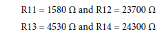
The resistor supplied on the circuit board is the value nearest EIA standard 0.1% resistor that is obtainable from and available with the suppliers. Thus, actual values of the resistor supplied on the board are as follows:
With these values supplied with the board, the offset errors due to the resistor values are as follows:

It is also possible to use combination of two 0.1% values to come closer to the calculated values minimize this offset error.
Total Receiver Circuit Accuracy
A good approximation of the total error contributed by the resistor tolerances is to assume that each of the critical resistors contributes equally to the total error. The four critical resistors are R11 or R13, R12 or R14, R6 and R10. Worst-case tolerance build up of 0.1% resistors yield a total resistor error of 0.4% maximum. If rss errors are assumed, the total rss error is 0.1√4 = 0.2%.
The maximum and rss errors due to the active components in the system using the A grade for AD8420 and B grade for levels of ADR02 are shown in the table below.
| Error Component | Error | Error Value | Error % FSR |
| ADR02-B | Offset | 0.06% | 0.01% |
| AD8420-A | Offset | 250 µV | 0.01% |
| AD8420-A |
Gain | 0.05% | 0.05% |
| RSS FS Offset | 0.014% | ||
| RSS FS Gain | 0.05% | ||
| RSS FS Error | 0.064% | ||
| Max FS Offset | 0.02% | ||
| Max FS Gain | 0.05% | ||
| Max FS Error | 0.07% |
Adding the worst case resistor tolerance error of 0.4% to the worst-case errors due to the active components yields:
Full Scale Error = 0.4% + 0.07% = 0.47%
These errors assume that ideal resistors were selected, and the errors resulted from their tolerances.
Actual error data for the receiver circuit is shown in Figure 5 and Figure 6 with VCC= 25 V. The total output error (%FSR) is calculated by taking the difference between the measured output voltage and the ideal output current, dividing by the FSR of the output voltage, and multiplying the result by 100.


A design support package for the EVAL-CN0314-EB1Z transmitter/receiver board including complete schematics, bill of materials, layout files, etc., can be found at http://www.analog.com/CN0314-DesignSupport.
Common Variations
The circuit is proven to work with good stability and accuracy with component values shown. Other voltage references and in-amp can be used in this configuration for other various applications for this circuit.
The AD8237, a micropower, zero drift, true rail-to-rail instrumentation amplifier can also be used for low supply voltage versions of this circuit configuration.
The ADR4550, high precision, low power, low noise voltage references can be used to replace the ADR02 for a low voltage supply applications.
Circuit Evaluation & Test
Equipment Required
- EVAL-CN0314-EB1Z evaluation board
- Agilent E3631A dual dc power supply or equivalent
- Yokogawa 2000 Precision DC Power Supply or equivalent.
- Agilent 3458 Precision Multimeter or equivalent
Test Setup Configuration and Tests
The circuit was tested using the test setup shown in Figure 7 and Figure 8. The Agilent 3631A was set to 25 V to serve as the power supply of the board. The Agilent 3458 Multimeter was used to measure the actual current or voltage output of the evaluation board. A photo of the EVAL-CN0314-EB1Z is shown in Figure 9.
For the test setup of the transmitter configuration (Figure 8), a Yokogawa 2000 Precision DC Source was used to generate a 0 V to 5 V or 0 V to 10 V differential input ranges. The S1 switch must be placed in the “V-I” position to configure the circuit as a transmitter.


For the test setup of the receiver configuration (Figure 9), a second EVAL-CN0314-EB1Z was used to produce a 4 mA to 20 mA input current. A precision current source can be used if desired. The S1 switch must be placed in the “I-V” position to configure the circuit as a receiver.


Switch and Jumper Settings for 4mA-to-20mA Transmitter
For the transmit configuration shown in Figure 1, Switch S1 should be put in the "V-I" position. Jumper P3 should be put in the "0-10V" position for an input range of 0V to 10V, and in the "0-5V" position for an imput range of 0V to 5V. See also the photo for evaluation board in Figure 9.
Switch and Jumper Settings for 4mA-to-20mA Receiver
For the receiver configuration shown in Figure 4, Switch S1 should be put in the "V-I" position. Jumper J4 should be put in the "0.2-2.3V" position for an output voltage of 0.2V to 2.3V, and in the "0.2-4.8V" position for an output voltage of 0.2V to 4.8V.See also the photo for evaluation board in Figure 9.