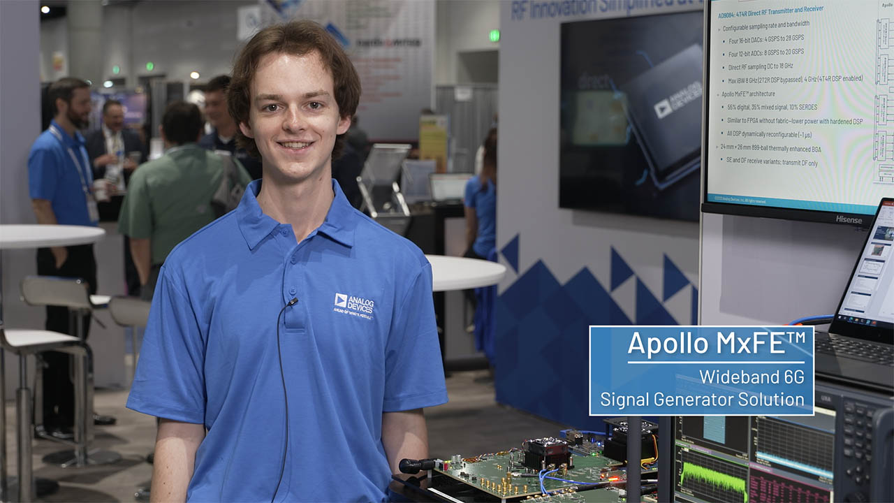
AD9084
RECOMMENDED FOR NEW DESIGNSApollo MxFE Quad, 16-Bit, 28GSPS RF DAC and Quad, 12-Bit, 20 GSPS RF ADC
- Part Models
- 3
- 1ku List Price
- Starting From $2012.50
Overview
- Reconfigurable mixed signal platform design
- 4 16-bit RF DACs and 4 12-bit RF ADCs (4T4R)
- Usable RF analog bandwidth to 18GHz
- Fast detect with low latency for fast AGC control
- Spectrum sniffer and monitor
- Signal monitor for slow AGC control
- Multiple loopback (ADC to DAC)
- Power amplifier downstream protection circuitry
- Maximum DAC/ADC sample rate up to 28GSPS/20GSPS
- Versatile digital features
- Maximum instantaneous bandwidth of 10GHz per channel (2T2R)
- Programmable FIR filters at full ADC and DAC sample rates
- Configurable fine and coarse DDCs and DUCs
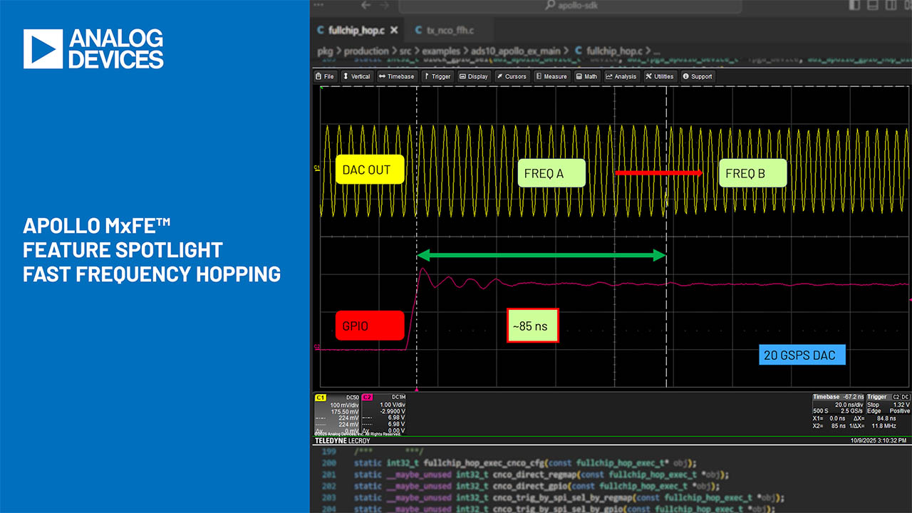
- Fast frequency hopping with profiles
- Dynamic configuration through SPI, HSCI, GPIO, or external trigger (TRIG)
- Programmable fractional data rate resampler from 1× to 2×
- JESD204B and JESD204C: 20Gbps and 28.21Gbps
- On-chip temperature monitoring unit
- Package: 24mm × 26mm, 899-ball BGA with 0.8mm pitch
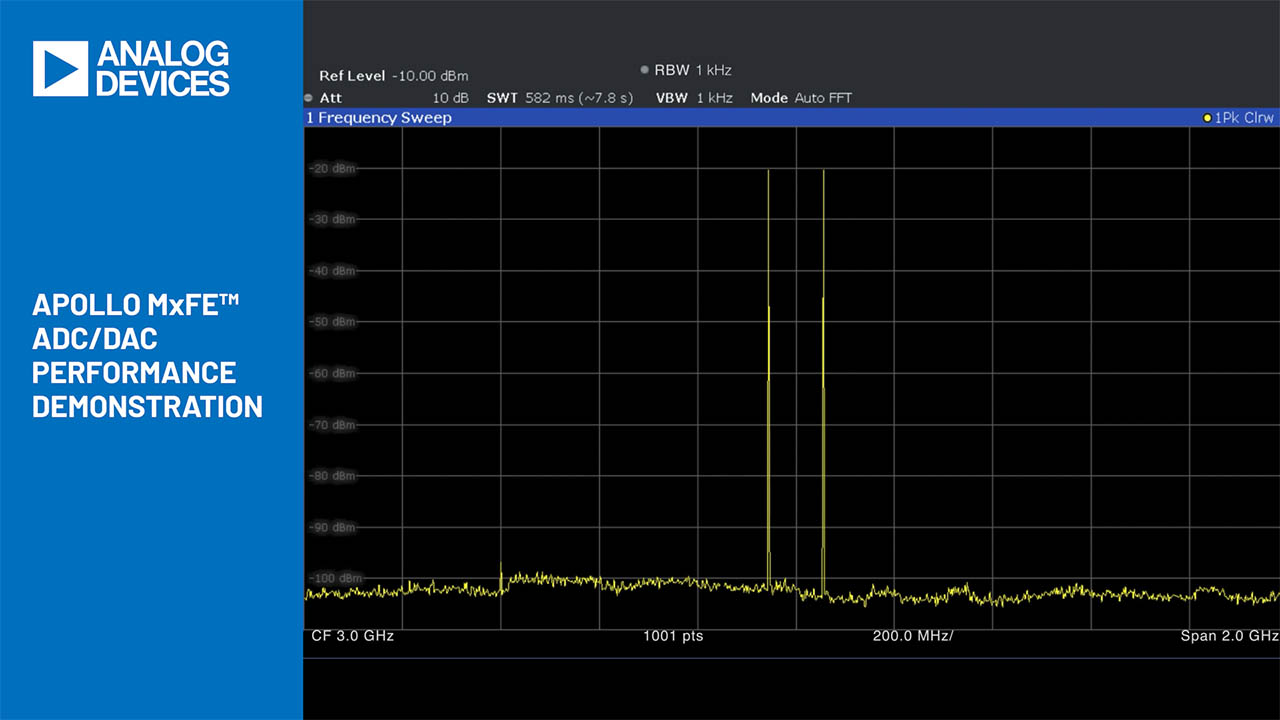
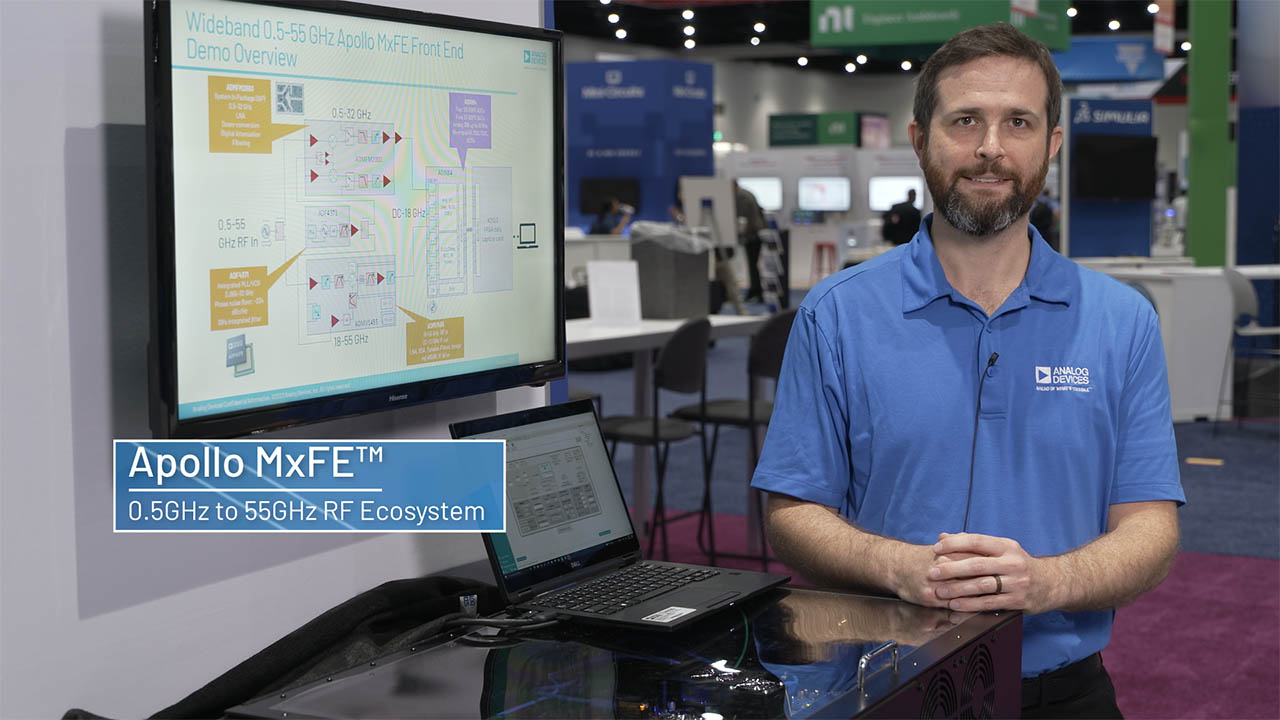
The mixed signal front-end (Apollo MxFE™ ) is a highly integrated device with a 16-bit, 28GSPS maximum sample rate, RF digital-to-analog converter (DAC) core, and 12-bit, 20GSPS maximum sample rate, RF analog-to-digital converter (ADC) core. The AD9084 supports four transmitter channels and four receiver channels. The AD9084 is well suited for applications requiring both wideband ADCs and DACs to process signal(s) having wide instantaneous bandwidth. The device features a 48 lane, 28.21Gbps JESD204C or 20Gbps JESD204B data transceiver port, an on-chip clock multiplier, and a digital signal processing (DSP) capability targeted at either wideband or multiband, direct to RF applications. The AD9084 also features a bypass mode that allows the full bandwidth capability of the ADC and/or DAC cores to bypass the DSP datapaths. The device also features low latency loopback and frequency hopping modes targeted at phased array radar systems and electronic warefare applications.
The AD9084 is available in a 24mm × 26mm, 899-ball BGA_ED.
Applications
- Radar and phase array systems
- Seeker front end
- Tactical defense radio infrastructure
- Electronic warfare and signal intelligence
- Wireless communications infrastructure
- Wireless communications test (5G mmWave, 5G C band, backhaul)
Thank you for showing interest in Apollo MxFE™ and our upcoming AD9084/AD9088 product release! Subscribe to stay on top of Apollo news, TODAY!
Documentation
Data Sheet 1
User Guide 2
Application Note 1
Technical Articles 22
Video 25


Device Drivers 4
FPGA Interoperability Reports 5
Product Selection Guide 1
3rd Party Solutions 1
Analog Dialogue 3
Video Series 1
Webcast 2
ADI has always placed the highest emphasis on delivering products that meet the maximum levels of quality and reliability. We achieve this by incorporating quality and reliability checks in every scope of product and process design, and in the manufacturing process as well. "Zero defects" for shipped products is always our goal. View our quality and reliability program and certifications for more information.
| Part Model | Pin/Package Drawing | Documentation | CAD Symbols, Footprints, and 3D Models |
|---|---|---|---|
| AD9084BBPZ-MX-DF-SW1 | BGA_ED | ||
| AD9084BBPZ-MX-DF-SW3 | BGA_ED | ||
| AD9084BBPZ-MX-DF-SW5 | BGA_ED |
This is the most up-to-date revision of the Data Sheet.
Software Resources
Device Drivers 5
- Prototyping Landing Page
- Linux driver
- AD908x GitHub Linux Driver Source Code
- HDL Reference Design
API Device Drivers 1
Device Application Programming Interface (API) C code drivers provided as reference code that allows the user to quickly configure the product using high-level function calls. The library acts as an abstraction layer between the application and the hardware. The API is developed in C99 to ensure agnostic processor and operating system integration. Customers can port this application layer code to their embedded systems by integrating their platform-specific code base to the API HAL layer.
To request this software package, go to the Software Request Form signed in with your MyAnalog account and under “Target Hardware” select “High Speed Data Converters” and choose the desired API product package. In addition, there are two SW packages available specifically for Apollo MxFE™. There is a PyApp/ACE evaluation package and there are FPGA bin files supporting various use cases. You will receive an email notification once the software is provided to you.
Evaluation Software 2
JESD204x Frame Mapping Table Generator
The JESD204x Frame Mapping Table Generator tool consists of two Windows executables that will allow the user to input any valid combination of JESD204x parameters (L, M, F, S, NP) in order to output a .csv file that illustrates the frame mapping of the JESD204x mode in table format. There is an executable that allows the user to input a single JESD204x mode and another, that allows the user to input the parameters for multiple JESD204x modes in a specified .csv format in order to output a .csv file that illustrates the frame mapping of each of the JESD204x modes that were input into separate tables.
JESD204 Interface Framework
Integrated JESD204 software framework for rapid system-level development and optimization
Hardware Ecosystem
| Parts | Product Life Cycle | Description |
|---|---|---|
| Clock ICs 1 | ||
| ADF4030 | RECOMMENDED FOR NEW DESIGNS | 10-Channel Precision Synchronizer |
| LDO Linear Regulators 2 | ||
| LTM4709 | RECOMMENDED FOR NEW DESIGNS | Triple 3A, Ultralow Noise, High PSRR, Ultrafast μModule Linear Regulator with Configurable Output Array |
| LT3094 | RECOMMENDED FOR NEW DESIGNS | −20V, 500mA, Ultralow Noise, Ultrahigh PSRR Negative Linear Regulator |
| Phase-Locked Loop (PLL) Synthesizers 2 | ||
| ADF4382 | RECOMMENDED FOR NEW DESIGNS | Microwave Wideband Synthesizer with Integrated VCO |
| ADF4382A | RECOMMENDED FOR NEW DESIGNS | 2.87GHz to 21GHz Fractional-N PLL/VCO for High Performance Converter Clocking Applications |
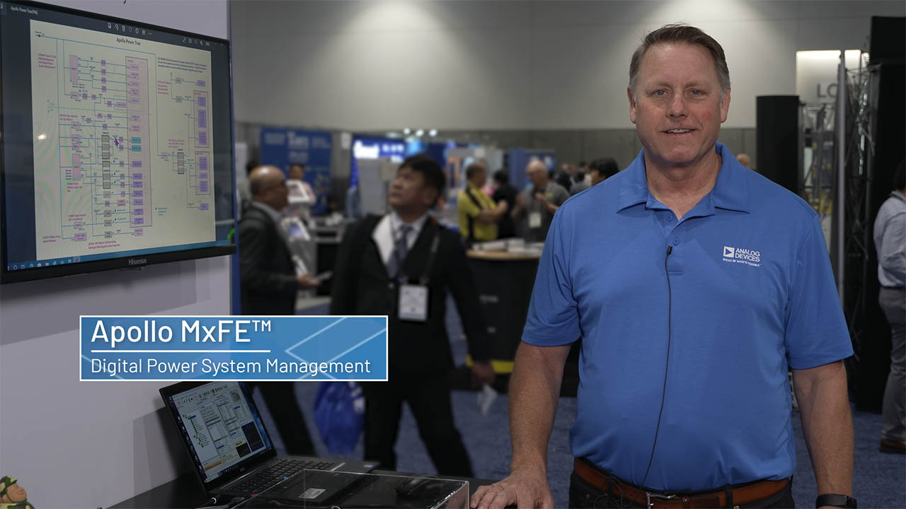
| Power System Management (PSM) & Sequencers 1 | ||
| LTC2977 | RECOMMENDED FOR NEW DESIGNS | 8-Channel PMBus Power System Manager Featuring Accurate Output Voltage Measurement |
| Switching Regulators & Controllers 3 | ||
| LT8627SP | RECOMMENDED FOR NEW DESIGNS | 18V/16A Step-Down Silent Switcher 3 with Ultralow Noise Reference |
| LTM4702 | RECOMMENDED FOR NEW DESIGNS | 16VIN, 8A Ultralow Noise Silent Switcher 3 μModule Regulator |
| LTM8074 | RECOMMENDED FOR NEW DESIGNS | 40VIN, 1.2A Silent Switcher µModule Regulator |
| Variable Gain Amplifiers (VGA) 2 | ||
| ADL6331 | RECOMMENDED FOR NEW DESIGNS | 0.38 GHz to 15 GHz TxVGA |
| ADL6332 | RECOMMENDED FOR NEW DESIGNS | 0.38 GHz to 15 GHz RxVGA |
Tools & Simulations
ADIsimPLL™
ADIsimPLL enables the rapid and reliable evaluation of new high performance PLL products from ADI. It is the most comprehensive PLL Synthesizer design and simulation tool available today. Simulations performed include all key non-linear effects that are significant in affecting PLL performance. ADIsimPLL removes at least one iteration from the design process, thereby speeding the design- to-market.
Open ToolFrequency Folding Tool
This tool illustrates the aliasing effects of an input signal and its harmonics when digitized by an ADC. The user can select single tone or a modulated carrier input signal and can observe aliasing in up to 10 Nyquist zones.
Open ToolCoherent Sampling Calculator
Calculate coherent sampling frequency and coherent input frequency
Open ToolData Conversion Calculator
Calculate ENOB, SNR, SINAD, THD.
Open ToolSNR/THD/SINAD Calculator
This calculator converts SNR, THD, and SINAD into ENOBs and noise. It also computes one of SNR, THD, or SINAD from the other two.
Open ToolClock & Timing Tools
Analog Devices provides design tools that work with our product portfolio to help engineers build critical clock and timing IC solutions for wired and wireless networks.
Open ToolAD9088 AMI Model
Design file package for the AD9084 and AD9088.
Open ToolThermal Models 1
High Speed Converter Toolbox for MATLAB
Open ToolS-Parameter 1
Evaluation Kits


ADS10-V1EBZ Evaluation Board
Resources


16Tx/16Rx Direct X-Band Sampled Phased-Array/RADAR/SATCOM Development Platform


ADMX7103-EBZ: 6G FR3 Radio Front-End
Resources
Software


Evaluating the AD9084 Apollo MxFE