CN0300


Overview
Design Resources
Design & Integration File
- Schematic
- Bill of Materials
- Gerber Files
- PADS Files
- Assembly Drawing
Evaluation Hardware
Part Numbers with "Z" indicate RoHS Compliance. Boards checked are needed to evaluate this circuit.
- EVAL-CN0300-EB1Z ($140.06) Complete Closed-Loop Precision Analog Microcontroller Thermocouple Measurement System with 4 mA to 20 mA Output
Features & Benefits
- T-type thermocouple measurement system, to loop powered 4-20mA output
- Typical temperature range of -200 C to +400 C
- Single chip solution using a Cortex processing core
- Cold junction compensation
Product Categories
Markets and Technologies
Parts Used
Documentation & Resources
-
MT-101: Decoupling Techniques2/14/2015PDF954 kB
-
MT-023: ADC Architectures IV: Sigma-Delta ADC Advanced Concepts and Applications2/14/2015PDF936 kB
-
MT-022: ADC Architectures III: Sigma-Delta ADC Basics2/14/2015PDF289 kB
-
MT-031: Grounding Data Converters and Solving the Mystery of "AGND" and "DGND"3/20/2009PDF144 kB
-
CN-0300: 12-Bit, 4-20mA Loop-Powered Thermocouple Measurement System Using ARM Cortex-M312/29/2013PDF379 kB
Circuit Function & Benefits
This circuit uses the ADuCM360 precision analog microcontroller in an accurate thermocouple temperature monitoring application and controls the 4 mA to 20 mA output current accordingly. The ADuCM360 integrates dual 24-bit sigma-delta (Σ-Δ) analog-to-digital converters (ADCs), dual programmable current sources, a 12-bit digital-to-analog converter (DAC), and a 1.2 V internal reference, as well as an ARM Cortex-M3 core, 126 kB flash, 8 kB SRAM, and various digital peripherals such as UART, timers, SPIs, and I2C interfaces.
In the circuit, the ADuCM360 is connected to a Type T thermocouple and a 100 Ω platinum resistance temperature detector (RTD). The RTD is used for cold junction compensation. The low power Cortex-M3 core converts the ADC readings to a real temperature value. The Type T temperature range supported is −200°C to +350°C, and this temperature range is converted to an output current range of 4 mA to 20 mA.


Circuit Description
The following features of the ADuCM360 are used in this application:
- The 12-bit DAC output with its flexible on-chip output buffer is used to control an external NPN transistor, BC548. By controlling the VBE voltage of this transistor, the current passing through a 47 Ω load resistor can be set to the desired value. When NPN mode is selected, the buffered on chip 1.2 V reference voltage is present on AIN8.
- The DAC is 12-bit monotonic; however, the accuracy of the DAC output is typically around 3 LSBs. In addition, the bi-polar transistor introduces linearity errors. To improve the accuracy of the DAC output and to eliminate offset and gain end-point errors, ADC0 measures, on AIN9, a feedback voltage reflecting the voltage across the load resistor (RLOAD). Based on this ADC0 reading, the DAC output is corrected by the source code. This provides ±0.5°C accuracy on the 4 mA to 20 mA output.
- The 24-bit Σ-Δ ADC with a PGA set for a gain of 32 in the software for the thermocouple and the RTD. ADC1 switches continuously between sampling the thermocouple and the RTD voltages.
- Programmable excitation current sources force a controlled current through the RTD. The dual current sources are configurable in steps from 0 μA to 2 mA. For this example, a 200 μA setting is used to minimize the error introduced by the RTD self-heating.
- An internal 1.2 V reference is provided for the ADC in the ADuCM360. When measuring the thermocouple voltage, the internal voltage reference is used due to its precision.
- An external voltage reference for the ADC in the ADuCM360. When measuring the RTD resistance, a ratiometric setup was used where an external reference resistor (RREF) was connected across the external VREF+ and VREF− pins. The on-chip reference input buffer is enabled because the reference source in this circuit is high impedance. The on-chip reference buffer means no external buffer is required to minimize input leakage effects.
- A bias voltage generator (VBIAS). The VBIAS function is used to set the thermocouple common-mode voltage to AVDD_Reg/2 (900 mV). Again, this removes the need for external resistors to set the thermocouple common-mode voltage.
- The ARM Cortex-M3 core. The powerful 32-bit ARM core with integrated 126 kB flash and 8 kB SRAM memory runs the user code that configures and controls the ADCs and converts the ADC conversions from the thermocouple and RTD inputs to a final temperature value. It also controls the DAC output and continuously monitors this DAC output using the closed-loop feedback from the voltage level on AIN9. For extra debug purposes, it also controls the communications over the UART/USB interface.
- The UART is used as the communication interface to the host PC. This is used to program the on-chip flash. It is also used as a debug port and for calibrating the DAC and ADC.
- Two external switches are used to force the part into its flash boot mode. By holding SD low and toggling the RESET button, the ADuCM360 enters boot mode instead of normal user mode. In boot mode, the internal flash can be reprogrammed through the UART interface.
- The J1 connector, an 8-pin dual-in-line connector, connects to the Analog Devices J-Link OB emulator that is provided with the CN0300 support hardware. This allows programming and debugging of this application board. See Figure 3.
Both the thermocouple and the RTD generate very small signals; therefore, a programmable gain amplifier (PGA) is required to amplify those signals.
The thermocouple used in this application is a Type T (copper-constantan) that has a temperature range of −200°C to +350°C. Its sensitivity is approximately 40 μV/°C, which means that the ADC in bipolar mode, with a PGA gain of 32, can cover the entire temperature range of the thermocouple.
The RTD was used for cold junction compensation. The particular one used in this circuit was a platinum 100 Ω RTD, Enercorp PCS 1.1503.1. It is available in a 0805, surface-mount package. This RTD has a temperature variation of 0.385 Ω/°C.
Note that the reference resistor, RREF, must be a precision 5.6 kΩ (±0.1%).
Construct the circuit on a multilayer printed circuit board (PCB) with a large area ground plane. Use proper layout, grounding, and decoupling techniques to achieve optimum performance (see Tutorial MT-031, Grounding Data Converters and Solving the Mystery of "AGND" and "DGND", Tutorial MT-101, Decoupling Techniques, and the ADuCM360TCZ Evaluation Board layout).


The Analog Devices J-Link OB emulator (USB-SWD/UART-EMUZ) supports the following:
- When plugged into a PC USB port, it can also be used to connect to a COM port (virtual serial port) on the PC. This is required for running the calibration routines.
- Provides SW (Serial Wire) debugging and programming for the ADuCM360.
- This USB port can be used to program the part using the UART-based downloader. Code Description
- Figure 4 shows a top view of the emulator board. J2 connector plugs into the EVAL-CN0300-EB1Z board. The J2 connector pinout is shown in Figure 5


For downloading and debugging, LK1, LK2, LK4, and LK6 must be inserted. LK3 and LK5 are required to communicate via UART. Required software for the J-Link OB is included in the software installation.
Note that the J-Link OB emulator replaces the J-Link Lite and related interface boards previously shipped with the ADuCM360 development system.
For more details, see UG-457, ADuCM360 Development Systems Getting Started Tutorial.
The link to the source code used to test the circuit can be found in the CN0300 Design Support Package located at http://www.analog.com/CN0300-DesignSupport. The source code uses the function libraries provided with the example code. Figure 6 shows the list of source files used in the project when viewed with the Keil μVision4 tools.

Figure 6. Source Files Viewed in μVision4
Calibration Section of Code
The compiler #define values, calibrateADC1 and calibrateDAC, can be adjusted to enable or disable calibration routines for the ADC and the DAC.
To calibrate either the ADC or the DAC, the Analog Devices J-Link OB emulator (USB-SWD/UART-EMUZ) must be connected to J1 and to the USB port on a PC. A COM port viewer program, such as HyperTerminal, can be used to view the calibration menus and step through the calibration routines.
When calibrating the ADC, the source code prompts the user to connect zero-scale and full-scale voltages to AIN2 and AIN3. Note that AIN2 is the positive input. On completion of the calibration routine, the new calibration values for the ADC1INTGN and ADC1OF registers are stored to the internal flash.
When calibrating the DAC, connect the VLOOP+ output through an accurate current meter. The first part of the DAC calibration routine calibrates the DAC to set a 4 mA output, and the second part of the DAC calibration routine calibrates the DAC to set a 20 mA output. The DAC code used to set a 4 mA and 20 mA output is stored to flash. The voltage measured at AIN9 for the final 4 mA and 20 mA settings is also recorded and saved to flash. Because the voltage at AIN9 is linearly related to the current flowing across RLOOP, these values are used to calculate the adjustment factor for the DAC. This closed-loop scheme means any linearity errors on the DAC and transistor based circuit are fine-tuned out using the on-chip 24-bit Σ-Δ ADC.
The UART is configured for a baud rate of 9600, 8 data bits, no parity, and no flow control. If the circuit is connected directly to a PC, a communication port viewing application, such as HyperTerminal, can be used to view the results sent by the program to the UART, as shown in Figure 7.
To enter the characters required by the calibration routines, type the required character in the viewing terminal and this character will be received by the ADuCM360 UART port.


Temperature Measurement Section of Code
To get a temperature reading, measure the temperature of the thermocouple and the RTD. The RTD temperature is converted to its equivalent thermocouple voltage via a look-up table (see the ISE, Inc., ITS-90 Table for Type T Thermocouple). These two voltages are added together to give the absolute value at the thermocouple.
First, the voltage measured between the two wires of the thermocouple (V1). The RTD voltage is measured, converted to a temperature via a look-up table, and then, this temperature is converted to its equivalent thermocouple voltage (V2). V1 and V2 are then added to give the overall thermocouple voltage, and this is then converted to the final temperature measurement.
For the thermocouple, temperatures for a fixed number of voltages are stored in an array. Temperature values in between are calculated using a linear interpolation between the adjacent points.
Figure 8 shows the error obtained when using ADC1 on the ADuCM360 to measure 52 thermocouple voltages over the full thermocouple operating range. The overall worst-case error is less than 1°C.


The RTD temperature is calculated using lookup tables and is implemented for the RTD the same way as for the thermocouple. Note that the RTD has a different polynomial describing its temperatures as a function of resistance.
For details on linearization and maximizing the performance of the RTD, refer to Application Note AN-0970, RTD Interfacing and Linearization Using an ADuC706x Microcontroller.
Temperature-to-Current Output Section of Code
Once the final temperature has been measured, set the DAC output voltage to the appropriate value that gives the required current across RLOOP. The input temperature range is expected to be −200°C to +350°C. The code sets the output current to 4 mA for −200°C and 20 mA for +350°C. The code implements a closed-loop scheme, as shown in Figure 9, where the feedback voltage on AIN9 is measured by ADC0, and this value is used to compensate the DAC output setting. The FineTuneDAC(void) function performs this correction.
For best results, calibrate the DAC before beginning performance testing of this circuit.


For debug purposes, the following strings are sent to the UART during normal operation (see Figure 10).


Common Variations
For a standard UART-to-RS-232 interface, the FT232R transceiver can be replaced with a device such as the ADM3202, which requires a 3 V power supply. For a wider temperature range, a different thermocouple can be used, such as a Type J. To minimize the cold junction compensation error, a thermistor can be placed in contact with the actual cold junction instead of on the PCB.
Instead of using the RTD and external reference resistor for measuring the cold junction temperature, an external digital temperature sensor can be used. For example, the ADT7410 can connect to the ADuCM360 via the I2C interface.
For more details on cold junction compensation, refer to Sensor Signal Conditioning, Analog Devices, Chapter 7, “Temperature Sensors.”
If isolation between the USB connector and this circuit is required, the ADuM3160/ADuM4160 isolation devices must be added.
Circuit Evaluation & Test
Current Output Measurements
The DAC and external-voltage-to-current-convertor circuit performance tests were all completed together.
A current meter was placed in series with the VLOOP+ connection, as shown in Figure 1. The meter used was a HP 34401A. The circuit performance when the initial calibration is performed and when using the closed-loop control of the VDAC output results in temperature values of 0.5°C being reported by the DAC output circuit. Nonlinearity errors from the DAC and the external transistor circuit are adjusted out thanks to the 24-bit ADC. Because temperature is a slow changing input parameter, this closed scheme is ideal for this application. Figure 11 shows the ideal DAC output in blue and the real DAC output with no closed-loop control (ADC0 is not used to compensate the DAC output). The error can be >10°C without closed-loop control.

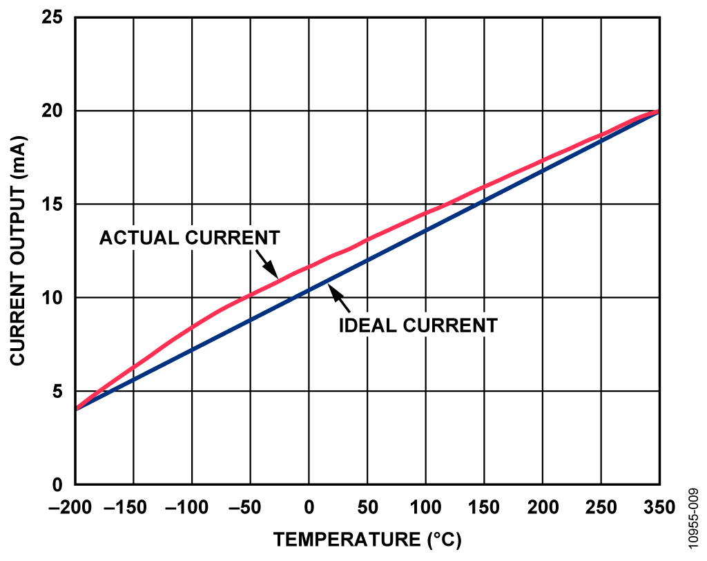
Figure 12 shows the same information when the closed-loop control is used as is recommended. The error is tiny, less than 0.5°C from the ideal value.


Thermocouple Measurement Test
The basic test setup is shown in Figure 13. The thermocouple is connected to J2.
Two methods were used to evaluate the performance of the circuit. Initially, the circuit was tested with the thermocouple attached to the board, and it was used to measure the temperature of an ice bucket. Then, it was used to measure the temperature of boiling water.
A Wavetek 4808 multifunction calibrator was used to fully evaluate the error, as shown in Figure 13. In this mode, the thermocouple was replaced with the calibrator as the voltage source. To evaluate the entire range of a Type T thermocouple, the calibrator was used to set the equivalent thermocouple voltage at 52 points between −200°C to +350°C for the negative and positive ranges of the T-type thermocouple (see the ISE, Inc., ITS-90 Table for Type T Thermocouple). Figure 8 shows the test results.
When doing performance checks and using the CN0300 circuit for normal operation, please ensure the J-Link OB emulator is unplugged from the EVAL-CN0300-EB1Z board—only use the J-Link OB when programming, calibrating and debugging the EVAL-CN0300-EB1Z board.


RTD Measurement Test
To evaluate the RTD circuit and linearization source code, the RTD on the board was replaced with an accurate, adjustable resistance source. The instrument used was the 1433-Z decade resistor. The RTD values are from 90 Ω to 140 Ω, which represents an RTD temperature range of −25°C to +114°C.
The test setup circuit for measuring the RTD is shown in Figure 14, and the error results for the RTD tests are shown in Figure 15.


Current Measurement Tests
When operating normally, the entire circuit consumes 2.25 mA typically. When held in a reset state, the entire circuit consumes less than 600 μA.
When doing performance checks and using the CN0300 circuit for normal operation, please ensure the J-Link OB emulator is unplugged from the EVAL-CN0300-EB1Z board—only use the J-Link OB when programming, calibrating and debugging the EVAL-CN0300-EB1Z board.
For more details on the current consumption figures for the ADuCM360, see Application Note AN-1111.