
Analog Devices RF and microwave components are available as drop-in X-MWblocks®
from Quantic™ X-Microwave.
AD8353
PRODUCTION1 MHz TO 2.7 GHz RF Gain Block
Part Details
- Fixed gain of 20 dB
- Operational frequency of 1 MHz to 2.7 GHz
- Linear output power up to 9 dBm
- Input/output internally matched to 50 Ω
- Temperature and power supply stable
- Noise figure: 5.3 dB
- Power supply: 3 V or 5 V
The AD8353 is a broadband, fixed-gain, linear amplifier that operates at frequencies from 1 MHz up to 2.7 GHz. It is intended for use in a wide variety of wireless devices, including cellular, broadband, CATV, and LMDS/MMDS applications.
By taking advantage of ADI’s high performance, complementary Si bipolar process, these gain blocks provide excellent stability over process, temperature, and power supply. This amplifier is single-ended and internally matched to 50 Ω with a return loss of greater than 10 dB over the full operating frequency range.
The AD8353 provides linear output power of 9 dBm with 20 dB of gain at 900 MHz when biased at 3 V and an external RF choke is connected between the power supply and the output pin. The dc supply current is 42 mA. At 900 MHz, the output third-order intercept (OIP3) is greater than 23 dBm and is 19 dBm at 2.7 GHz.
The noise figure is 5.3 dB at 900 MHz. The reverse isolation (S12) is −36 dB at 900 MHz and −30 dB at 2.7 GHz.
The AD8353 can also operate with a 5 V power supply; in which case, no external inductor is required. Under these conditions, the AD8353 delivers 8 dBm with 20 dB of gain at 900 MHz. The dc supply current is 42 mA. At 900 MHz, the OIP3 is greater than 22 dBm and is 19 dBm at 2.7 GHz. The noise figure is 5.6 dB at 900 MHz. The reverse isolation (S12) is −35 dB.
The AD8353 is fabricated on ADI’s proprietary, high performance, 25 GHz, Si complementary, bipolar IC process. The AD8353 is available in a chip scale package that uses an exposed paddle for excellent thermal impedance and low impedance electrical connection to ground. It operates over a −40°C to +85°C temperature range, and an evaluation board is also available.
Applications
- VCO buffers
- General Tx/Rx amplification
- Power amplifier predrivers
- Low power antenna drivers
Documentation
Data Sheet 1
Application Note 3
Evaluation Design File 1
Product Selection Guide 1
This is the most up-to-date revision of the Data Sheet.
Software Resources
Can't find the software or driver you need?
Request a Driver/SoftwareTools & Simulations
S-Parameter 1
ADIsimPLL™
ADIsimPLL enables the rapid and reliable evaluation of new high performance PLL products from ADI. It is the most comprehensive PLL Synthesizer design and simulation tool available today. Simulations performed include all key non-linear effects that are significant in affecting PLL performance. ADIsimPLL removes at least one iteration from the design process, thereby speeding the design- to-market.
Open ToolADIsimRF
ADIsimRF is an easy-to-use RF signal chain calculator. Cascaded gain, noise, distortion and power consumption can be calculated, plotted and exported for signal chains with up to 50 stages. ADIsimRF also includes an extensive data base of device models for ADI’s RF and mixed signal components.
Open ToolSys-Parameter Models for Keysight Genesys
Sys-Parameter models contain behavioral parameters, such as P1dB, IP3, gain, noise figure and return loss, which describe nonlinear and linear characteristics of a device.
Open ToolEvaluation Kits
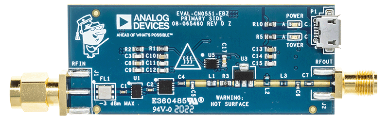
AD8353 Evaluation Board
Resources
Reference Designs


USB-Powered, 433.92 MHz RF Power Amplifier with Overtemperature Management