AD9250
RECOMMENDED FOR NEW DESIGNS14-Bit, 170 MSPS/250 MSPS, JESD204B, Dual Analog-to-Digital Converter
- Part Models
- 4
- 1ku List Price
- Starting From $93.08
Part Details
- JESD204B Subclass 0 or Subclass 1 coded serial digital outputs
- Signal-to-noise ratio (SNR) = 70.6 dBFS at 185 MHz AIN and 250 MSPS
- Spurious-free dynamic range (SFDR) = 88 dBc at 185 MHz AIN and 250 MSPS
- Total power consumption: 711 mW at 250 MSPS
- 1.8 V supply voltages
- Integer 1-to-8 input clock divider
- Sample rates of up to 250 MSPS
- IF sampling frequencies of up to 400 MHz
- Internal analog-to-digital converter (ADC) voltage reference
- Flexible analog input range
- 1.4 V p-p to 2.0 V p-p (1.75 V p-p nominal)
- ADC clock duty cycle stabilizer (DCS)
- 95 dB channel isolation/crosstalk
- Serial port control
- Energy saving power-down modes
The AD9250 is a dual, 14-bit ADC with sampling speeds of up to 250 MSPS. The AD9250 is designed to support communications applications where low cost, small size, wide bandwidth, and versatility are desired.
The ADC cores feature a multistage, differential pipelined architecture with integrated output error correction logic. The ADC cores feature wide bandwidth inputs supporting a variety of user-selectable input ranges. An integrated voltage reference eases design considerations. A duty cycle stabilizer is provided to compensate for variations in the ADC clock duty cycle, allowing the converters to maintain excellent performance. The JESD204B high speed serial interface reduces board routing requirements and lowers pin count requirements for the receiving device.
By default, the ADC output data is routed directly to the two JESD204B serial output lanes. These outputs are at CML voltage levels. Four modes support any combination of M = 1 or 2 (single or dual converters) and L = 1 or 2 (one or two lanes). For dual ADC mode, data can be sent through two lanes at the maximum sampling rate of 250 MSPS. However, if data is sent through one lane, a sampling rate of up to 125 MSPS is supported. Synchronization inputs (SYNCINB± and SYSREF±) are provided.
Flexible power-down options allow significant power savings, when desired. Programmable overrange level detection is supported for each channel via the dedicated fast detect pins.
Programming for setup and control are accomplished using a 3-wire SPI-compatible serial interface.
The AD9250 is available in a 48-lead LFCSP and is specified over the industrial temperature range of −40°C to +85°C.
Product Highlights
- Integrated dual, 14-bit, 170 MSPS/250 MSPS ADC.
- The configurable JESD204B output block supports up to 5 Gbps per lane.
- An on-chip, phase-locked loop (PLL) allows users to provide a single ADC sampling clock; the PLL multiplies the ADC sampling clock to produce the corresponding JESD204B data rate clock.
- Support for an optional RF clock input to ease system board design.
- Proprietary differential input maintains excellent SNR performance for input frequencies of up to 400 MHz.
- Operation from a single 1.8 V power supply.
- Standard serial port interface (SPI) that supports various product features and functions such as controlling the clock DCS, power-down, test modes, voltage reference mode, over range fast detection, and serial output configuration.
Applications
- Diversity radio systems
- Multimode digital receivers (3G)
- TD-SCDMA, WiMAX, W-CDMA, CDMA2000, GSM, EDGE, LTE
- DOCSIS 3.0 CMTS upstream receive paths
- HFC digital reverse path receivers
- I/Q demodulation systems
- Smart antenna systems
- Electronic test and measurement equipment
- Radar receivers
- COMSEC radio architectures
- IED detection/jamming systems
- General-purpose software radios
- Broadband data applications
Documentation
Data Sheet 1
User Guide 1
Technical Articles 11
Evaluation Design File 2
Informational 1
FPGA Interoperability Reports 3
Device Drivers 3
Rarely Asked Question Page 1
Analog Dialogue 1
Webcast 3
ADI has always placed the highest emphasis on delivering products that meet the maximum levels of quality and reliability. We achieve this by incorporating quality and reliability checks in every scope of product and process design, and in the manufacturing process as well. "Zero defects" for shipped products is always our goal. View our quality and reliability program and certifications for more information.
| Part Model | Pin/Package Drawing | Documentation | CAD Symbols, Footprints, and 3D Models |
|---|---|---|---|
| AD9250BCPZ-170 | 48-Lead LFCSP (7mm x 7mm x 0.75mm w/ EP) | ||
| AD9250BCPZ-250 | 48-Lead LFCSP (7mm x 7mm x 0.75mm w/ EP) | ||
| AD9250BCPZRL7-170 | 48-Lead LFCSP (7mm x 7mm x 0.75mm w/ EP) | ||
| AD9250BCPZRL7-250 | 48-Lead LFCSP (7mm x 7mm x 0.75mm w/ EP) |
This is the most up-to-date revision of the Data Sheet.
Software Resources
FPGA/HDL 2
Device Drivers 3
Evaluation Software 2
JESD204x Frame Mapping Table Generator
The JESD204x Frame Mapping Table Generator tool consists of two Windows executables that will allow the user to input any valid combination of JESD204x parameters (L, M, F, S, NP) in order to output a .csv file that illustrates the frame mapping of the JESD204x mode in table format. There is an executable that allows the user to input a single JESD204x mode and another, that allows the user to input the parameters for multiple JESD204x modes in a specified .csv format in order to output a .csv file that illustrates the frame mapping of each of the JESD204x modes that were input into separate tables.
JESD204 Interface Framework
Integrated JESD204 software framework for rapid system-level development and optimization
Can't find the software or driver you need?
Hardware Ecosystem
| Parts | Product Life Cycle | Description |
|---|---|---|
| Clock Distribution Devices 3 | ||
| AD9513 | RECOMMENDED FOR NEW DESIGNS | 800 MHz Clock Distribution IC, Dividers, Delay Adjust, Three Outputs |
| AD9514 | RECOMMENDED FOR NEW DESIGNS | 1.6 GHz Clock Distribution IC, Dividers, Delay Adjust, Three Outputs |
| AD9515 | RECOMMENDED FOR NEW DESIGNS | 1.6 GHz Clock Distribution IC, Dividers, Delay Adjust, Two Outputs |
| Clock Generation Devices 9 | ||
| AD9510 | RECOMMENDED FOR NEW DESIGNS | 1.2 GHz Clock Distribution IC, PLL Core, Dividers, Delay Adjust, Eight Outputs |
| AD9511 | RECOMMENDED FOR NEW DESIGNS | 1.2 GHz Clock Distribution IC, PLL Core, Dividers, Delay Adjust, Five Outputs |
| AD9512 | RECOMMENDED FOR NEW DESIGNS | 1.2 GHz Clock Distribution IC, Two 1.6 GHz Inputs, Dividers, Delay Adjust, Five Outputs |
| AD9525 | RECOMMENDED FOR NEW DESIGNS | Low Jitter Clock Generator Eight LVPECL Outputs |
| AD9516-3 | RECOMMENDED FOR NEW DESIGNS | 14-Output Clock Generator with Integrated 2.0 GHz VCO |
| AD9516-4 | RECOMMENDED FOR NEW DESIGNS | 14-Output Clock Generator with Integrated 1.6 GHz VCO |
| AD9523 | NOT RECOMMENDED FOR NEW DESIGNS | 14-Output, Low Jitter Clock generator |
| AD9523-1 | RECOMMENDED FOR NEW DESIGNS | Low Jitter Clock Generator with 14 LVPECL/LVDS/HSTL/29 LVCMOS Outputs |
| AD9524 | NOT RECOMMENDED FOR NEW DESIGNS | 6 Output, Dual Loop Clock Generator |
| Digital Control VGAs 2 | ||
| ADL5202 | Obsolete | Wide Dynamic Range, High Speed, Digitally Controlled VGA |
| AD8376 | RECOMMENDED FOR NEW DESIGNS | Ultralow Distortion IF Dual VGA |
| Fully Differential Amplifiers 2 | ||
| ADL5562 | RECOMMENDED FOR NEW DESIGNS | 3.3 GHz Ultralow Distortion RF/IF Differential Amplifier |
| ADL5565 | RECOMMENDED FOR NEW DESIGNS |
6 GHz Ultrahigh Dynamic Range Differential Amplifier |
| Single-Ended to Differential Amplifiers 3 | ||
| ADA4930-2 | RECOMMENDED FOR NEW DESIGNS | Ultralow Noise Drivers for Low Voltage ADCs |
| ADA4927-2 | RECOMMENDED FOR NEW DESIGNS | Ultralow Distortion Current Feedback Differential ADC Driver |
| ADA4938-2 | RECOMMENDED FOR NEW DESIGNS | Ultralow Distortion Differential ADC Driver (Dual) |
Tools & Simulations
Virtual Eval - BETA
Virtual Eval is a web application to assist designers in product evaluation of ADCs, DACs, and other ADI products. Using detailed models on Analog’s servers, Virtual Eval simulates crucial part performance characteristics within seconds. Configure operating conditions such as input tones and external jitter, as well as device features like gain or digital down-conversion. Performance characteristics include noise, distortion, and resolution, FFTs, timing diagrams, response plots, and more.
Open ToolAD9250 AMI Model
Open ToolADC Companion Transport Layer RTL Code Generator Tool
This command line executable tool generates a Verilog module which implements the JESD204 receive transport layer. The user specifies in a configuration file one or more modes to be supported by the transport layer module. These modes are defined as a set of JESD204 parameter values: L, M, F, S, N', and CF. The transport layer converts JESD204 lane data output from a JESD204 link layer IP to a data bus with a fixed width, containing interleaved virtual converter samples. Both JESD204B and JESD204C link layers are supported.
Open ToolVisual Analog
For designers who are selecting or evaluating high speed ADCs, VisualAnalog™ is a software package that combines a powerful set of simulation and data analysis tools with a user-friendly graphical interface.
Open ToolADIsimRF
ADIsimRF is an easy-to-use RF signal chain calculator. Cascaded gain, noise, distortion and power consumption can be calculated, plotted and exported for signal chains with up to 50 stages. ADIsimRF also includes an extensive data base of device models for ADI’s RF and mixed signal components.
Open ToolAD9250 Simulink ADIsimADC Model
Open ToolEvaluation Kits


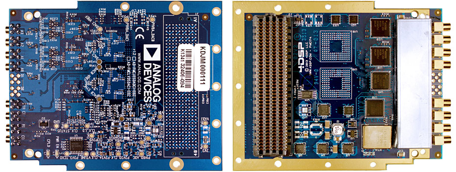
AD9250 Evaluation Board
Resources
AD-FMCJESDADC1-EBZ Rapid Development Board


FPGA Based Data Capture Kit