摘要
In many thermal applications, it may be desired to utilize multiple temperature sensors, placed in different physical locations, to monitor the operating temperatures in predefined 'zones' within the system. To accommodate this desire, many thermal products have the added flexibility of user-defined slave addressing.
A similar version was published in the March 2014 issue of Electronics Maker magazine.
Traditionally, most ICs incorporating the Philips® I2C I/O protocol have a fixed (factory-defined) slave address for use during communications. In many thermal applications, however, it may be desirable to utilize multiple temperature sensors, placed in different physical locations, to monitor the operating temperatures in predefined "zones" within the system. To accommodate this while minimizing CPU resources allocated for communications functions, many thermal products have the added flexibility of user-defined slave addressing. This user-defined function uses an additional input pin (or pins) that allows mapping of a specific sensor to a schematically defined slave address.
Categorizing the thermal products by its I/O multidrop capability results in three fundamental variations of the options for user-defined slave addressing:
Input-Level Defined. The condition of the address input pin can be controlled by a simple hardware definition (i.e., resistor placement) or by a dynamic CPU resource. Standard digital logic input levels (VIH/VIL) utilized on SCL and SDA can also be applied to the address input pin(s).
Figure 1 depicts a typical I2C resistor pullup scheme where the I2C master's resource is defined as open drain, and the default ADD pin state is Logic 1. The desired decode (ADD input bias) must be presented prior to the associated START signal whenever this slave is to be accessed; it should remain stable until after the associated STOP has been issued.
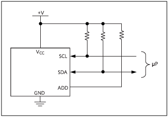
Figure 1. Input-level-defined addressing as implemented in the DS1621, DS75, or MAX6634 temp sensors. When this function is used, then multiple temperature devices like these can have their own slave address.
Input-level-defined components actively decode the address input pin(s) bias to determine the present slave address. On devices with an optional ADD pin to decode states of SDA or SCL, it is recommended that ADD be directly connected to that desired pin. Maximum signal margin is achieved by using full-rail address pin conditioning. When defining the address pin(s) conditions in hardware, use low-ohmic-value pullup/pulldown resistors (< 1kΩ).
Pin-State Defined. The address input pin condition must be controlled by the hardware definition (at PCB assembly). The components in this category have three or more variations of possible slave addresses, including a unique decode for cases where the input pin(s) may be left in an unconnected condition.
Figure 2 depicts a typical I2C address pin definition to ground. If ADD is to be defined by a power supply, the pin should be directly connected to the desired supply rail. (Use 0Ω to either V+ or GND.)
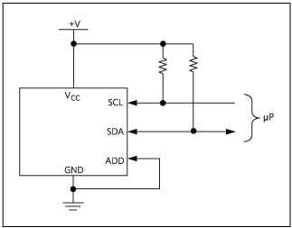
Figure 2. Pin-state-defined addressing, as implemented in the MAX6650 or MAX6681 temperature sensors, allows for definition of the address pin with local, direct connections.
Pins defined for "No Connection" should not have any external components or traces contacting those input pads. Figure 3 shows an improper placement of a resistor-divider, here attempting to hold the ADD input at (V+/2). If this pin conditioning is selected, be aware that downstream assembly artifacts (e.g., flux residue, moisture, adjacent digital traces, etc.) can negatively impact the operation of the intended address decoding. Use this unconnected option when there is no other choice available.
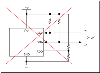
Figure 3. Do not use pullup or pulldown resistors on a "No Connection" pin configuration.
Pin-state-defined components operate similar to the input-level-defined designs, with the added complexity of a third (or sometimes fourth) variation of input conditioning (e.g., a float, resistor to GND, etc.). The components in this category are, therefore, much more sensitive to potential address miss-selection, noise coupling from adjacent traces, assembly processing (e.g., surface leakage paths from residual contaminants), or changes in raw silicon processing.
Pins defined to decode a high logic level should be directly connected (i.e., 0Ω to the device power supply. Pins defined to decode a low logic level should be directly connected (i.e., 0Ω to the board ground. Pins defined to decode a resistor to GND may require 5% external component tolerancing. Refer to the product's specifications for more details.
Ordering Defined. A specific ordering variant (i.e., a specific variation of a part's build of materials, BOM) is required so each unique slave address can be utilized. The advantage in this part-number-specific approach is noise immunity in the application. There may also be a disadvantage in the increased procurement/assembly complexity due to handling placement-critical variations of the same chip.
Figure 4 depicts a simplified connection scheme utilizing eight unique DS1775 digital thermometer ordering variants.
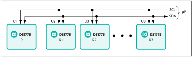
Figure 4. Ordering-defined addressing is implemented in the DS1775 and MAX6697 temperature sensors.
The ordering-defined components provide the most electrically robust solution for multichip placements, as there are no additional package pins or signals that must be controlled. But as initially noted, this solution requires a unique BOM and placement requirement on a per-socket basis.
In summary, the need for multidrop thermal sensing is based upon the specific system's temperature-monitoring requirements and a general desire to minimize the CPU resources dedicated to intercomponent I/O. We discussed three variations of multidrop implementations that are available in several temperature sensors and digital thermometers and thermostats offered in Maxim's Thermal Management product line.We also provided some guidance on implementation concerns for each variation.
关联至此文章
最新视频 21


