ADL8143
推荐用于新设计8 GHz 至 14 GHz,低噪声放大器
- 产品模型
- 4
产品详情
- 单正电源(自偏置)典型值:1.5 V 和 35 mA
- RBIAS 漏极电流调节引脚
- 增益:8 GHz 至 10 GHz 范围内为 28.5 dB
- 噪声指数:8 GHz 至 10 GHz 范围内为 1 dB
- 扩展的工作温度范围:−55°C 至 +125°C
- 内部匹配的和交流耦合的
- 符合 RoHS 标准的 2 mm x 2 mm、8 引脚 LFCSP 封装
ADL8143 是一款低噪声放大器 (LNA),工作频率为 8 GHz 至 14 GHz。8 GHz 至 10 GHz 范围内的典型增益、噪声系数、1 dB 压缩的输出功率 (OP1dB) 和输出三阶截距 (OIP3) 分别为 28.5 dB、1 dB、7.5 dBm 和 19.5 dBm。标称静态电流 (IDQ) 可以调整,在 1.5 V 电源电压 (VDD) 下为 35 mA。ADL8143 还具有交流耦合且内部匹配至 50 Ω 的输入和输出。
ADL8143 采用符合 RoHS 标准的 2 mm × 2 mm、8 引脚引线框架芯片级封装 [LFCSP],额定工作温度范围为 −55°C 至 +125°C。
应用
- 卫星通信
- 雷达
- 电信
参考资料
数据手册 2
用户手册 1
应用笔记 2
高剂量率辐射报告 1
ADI 始终高度重视提供符合最高质量和可靠性水平的产品。我们通过将质量和可靠性检查纳入产品和工艺设计的各个范围以及制造过程来实现这一目标。出货产品的“零缺陷”始终是我们的目标。查看我们的质量和可靠性计划和认证以了解更多信息。
| 产品型号 | 引脚/封装图-中文版 | 文档 | CAD 符号,脚注和 3D模型 |
|---|---|---|---|
| ADL8143ACPZN | 8-lead LFCSP 2 mm × 2 mm × 0.85 | ||
| ADL8143ACPZN-CSL | 8-lead LFCSP 2 mm × 2 mm × 0.85 | ||
| ADL8143ACPZN-R7 | 8-lead LFCSP 2 mm × 2 mm × 0.85 | ||
| ADL8143ACPZN-R7-CSL | 8-lead LFCSP 2 mm × 2 mm × 0.85 |
这是最新版本的数据手册
软件资源
找不到您所需的软件或驱动?
申请驱动/软件工具及仿真模型
S-参数 1
评估套件
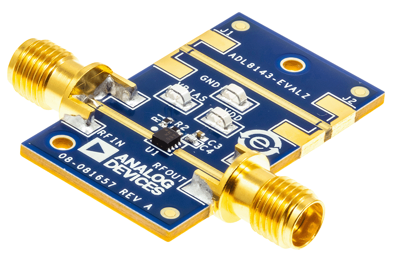
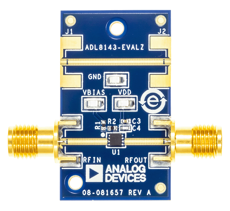
Evaluating the ADL8143 GaAs, pHEMT, MMIC, Low Noise Amplifier, 8 GHz to 14 GHz
资料
最新评论
需要发起讨论吗? 没有关于 ADL8143的相关讨论?是否需要发起讨论?
在EngineerZone®上发起讨论