LTC3204

製造中

2×2 DFNの低ノイズ安定化チャージポンプ

製品モデル
8
1Ku当たりの価格
最低価格:$2.09
利用上の注意

アナログ・デバイセズ社は、提供する情報が正確で信頼できるものであることを期していますが、その情報の利用に関して、あるいはその利用によって生じる第三者の特許やその他の権利の侵害に関して一切の責任を負いません。また、アナログ・デバイセズ社の特許または特許の権利の使用を明示的または暗示的に許諾するものでもありません。仕様は予告なしに変更する場合があります。本紙記載の商標および登録商標は、各社の所有に属します。


本データシートの英語以外の言語への翻訳はユーザの便宜のために提供されるものであり、リビジョンが古い場合があります。最新の内容については、必ず最新の英語版をご参照ください。

なお、日本語版のデータシートは基本的に「Rev.0」(リビジョン0)で作成されています。そのため、英語版が後に改訂され、複数製品のデータシートがひとつに統一された場合、同じ「Rev.0」の日本語版のデータシートが異なる製品のデータシートとして表示されることがあります。たとえば、「ADM3307E」の場合、日本語データシートをクリックすると「ADM3311E」が表示されます。これは、英語版のデータシートが複数の製品で共有できるように1本化され、「ADM3307E/ADM3310E/ADM3311E/ADM3312E/ADM3315E」(Rev.G)と改訂されたからで、決して誤ってリンクが張られているわけではありません。和文化されたデータシートを少しでも有効に活用していただくためにこのような方法をとっておりますので、ご了解ください。

Viewing:

製品の詳細

  • 3.3Vまたは5V固定出力
  • VIN範囲:
    • 1.8V~4.5V(LTC3204-3.3 /LTC3204B-3.3)
    • 2.7V~5.5V(LTC3204-5/ LTC3204B-5)
  • 出力電流
    • 最大150mA(LTC3204-5/ LTC3204B-5)
    • 最大50mA(LTC3204-3.3/LTC3204B-3.3)
  • IQ = 48μAの自動バーストモード動作(LTC3204-3.3/ LTC3204-5)
  • あらゆる負荷で固定周波数動作(LTC3204B-3.3/ LTC3204B-5)
  • 低ノイズ固定周波数(1.2MHz)動作
  • ソフトスタート機能により、突入電流を制限
  • シャットダウン時に入力から負荷を切断
  • シャットダウン電流:<1μA
  • 短絡/熱保護機能
  • 6ピン2mm x 2mm DFNパッケージ
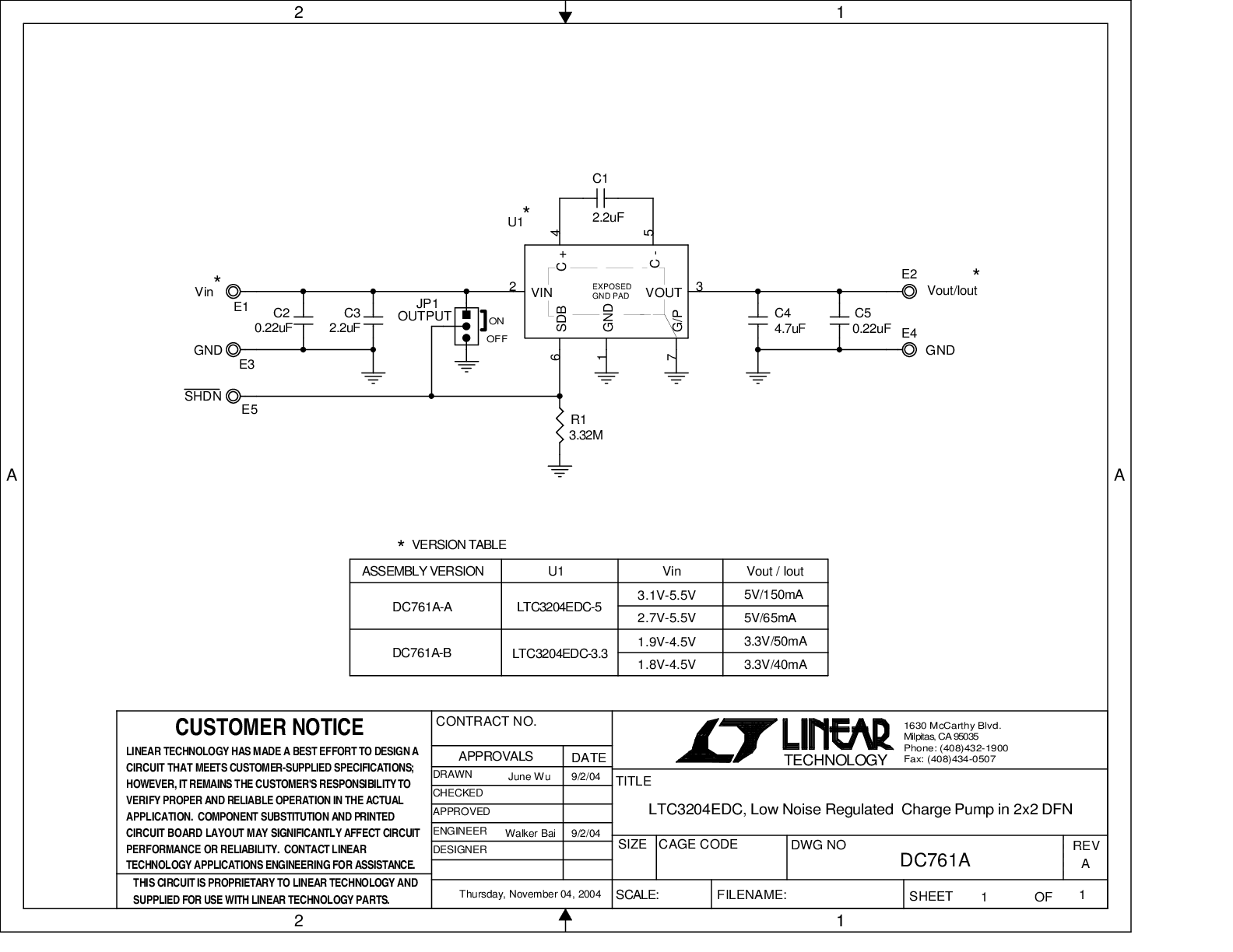
LTC3204
2×2 DFNの低ノイズ安定化チャージポンプ
Output Ripple vs Load Current Product Package 1
myAnalogに追加

myAnalogの製品セクション(通知受け取り)、既存/新規プロジェクトに製品を追加する。

新規プロジェクトを作成
質問する
サポート

アナログ・デバイセズのサポート・ページはアナログ・デバイセズへのあらゆるご質問にお答えするワンストップ・ポータルです。


ドキュメント

データシート 1

信頼性データ 1

ユーザ・ガイド 2

データシート

これは最新改訂バージョンのデータシートです。

さらに詳しく
myAnalogに追加

myAnalogの製品セクション(通知受け取り)、既存/新規プロジェクトに製品を追加する。

新規プロジェクトを作成

ツールおよびシミュレーション

LTspice

LTspice®は、無料で提供される強力で高速な回路シミュレータと回路図入力、波形ビューワに改善を加え、アナログ回路のシミュレーションを容易にするためのモデルを搭載しています。


評価用キット

eval board
DC916A-B

LTC3204BEDC-3.3 Demo Board | Low Noise Regulated Charge Pump in 2x2 DFN, VIN = 1.8V to 4.5V, VOUT = 3.3V/(40 to 50mA Max)

製品詳細

Demonstration circuit 916 is a low noise regulated charge pump featuring the LTC3204B (constant frequency switching) in the 2X2 DFN package. There are two assembly versions, DC916A-A and DC916A-B for the LTC3204B-5 (5V output) and LTC3204B-3.3 (3.3V output) respectively. The DC916A-B produces a regulated 3.3V output from a 1.8V to 4.5V input. The guaranteed output current is 50mA from VIN between 1.9V and 4.5V, and 40mA for VIN less than 1.9V.


The circuit requires only three tiny 0603 surface mount capacitors and uses minimal board space. No inductor or diodes are needed. The circuit features automatic Burst Mode® operation at light loads to maintain low supply current.

eval board
DC761A-B

LTC3204EDC-3.3 Demo Board | Low Noise Regulated Charge Pump in 2 × 2 DFN, Burst Mode, VIN = 1.8V to 4.5V, VOUT = 3.3V/(40mA to 50mA Max)

製品詳細

Demonstration circuit 761 is a low noise regulated charge pump featuring the LTC3204 (Burst Mode operation) in the 2 × 2 DFN package. There are two assembly versions, DC761A-A and DC761A-B for the LTC3204-5 (5V output) and LTC3204-3.3 (3.3V output) respectively. The DC761A-B produces a regulated 3.3V output from a 1.8V to 4.5V input. The guaranteed output current is 50mA from VIN between 1.9V and 4.5V, and 40mA for VIN less than 1.9V.


The circuit requires only three tiny 0603 surface mount capacitors and uses minimal board space. No inductor or diodes are needed. The circuit features automatic Burst Mode® operation at light loads to maintain low supply current.

eval board
DC761A-A

LTC3204EDC-5デモ・ボード | 低ノイズ安定化チャージ・ポンプ、2x2 DFN、バースト・モード、VIN = 2.7V–5.5V、VOUT = 5V/(65–150mA)

製品詳細

デモ回路761は、2x2 DFNパッケージにLTC3204(バースト・モード動作)を搭載した低ノイズ安定化チャージ・ポンプです。2つのアセンブリ・バージョンがあり、DC761A-AがLTC3204-5(5V出力)用、DC761A-BがLTC3204-3.3(3.3V出力用)です。DC761A-Aは、2.7V~5.5V入力から安定化された5V出力を生成します。確保する出力負荷電流は、VINが3.1V~5.5Vの場合は150mA、VINが3.1V未満の場合は65mAです。DC761A-Bは、1.8V~4.5V入力から安定化された3.3V出力を生成します。確保する出力負荷電流は、VINが1.9V~4.5Vの場合は50mA、VINが1.9V未満の場合は40mAです。


この回路で必要なのは、小型の0603表面実装型コンデンサ3個のみで、最小限の基盤スペースしか使用しません。インダクタやダイオードは不要です。回路は、軽負荷時に低電源電流を維持する自動Burst Mode®(バースト・モード)動作を備えています。


eval board
DC916A-A

LTC3204BEDC-5 Demo Board | Low Noise Regulated Charge Pump 2x2 DFN, VIN = 2.7V to 5.5V, VOUT = 5V/(65 to 150mA Max)

製品詳細

Demonstration circuit 916 is a low noise regulated charge pump featuring the LTC3204B (constant frequency operation) in the 2X2 DFN package. There are two assembly versions, DC916A-A and DC916A-B for the LTC3204B-5 (5V output) and LTC3204B-3.3 (3.3V output) respectively. The DC916A-A produces a regulated 5V output from a 2.7V to 5.5V input. The guaranteed output load current is 150mA for VIN between 3.1V and 5.5V, and 65mA for VIN less than 3.1V.


The circuit requires only three tiny 0603 surface mount capacitors and uses minimal board space. No inductor or diodes are needed. The circuit features automatic Burst Mode® operation at light loads to maintain low supply current.

DC916A-B
LTC3204BEDC-3.3 Demo Board | Low Noise Regulated Charge Pump in 2x2 DFN, VIN = 1.8V to 4.5V, VOUT = 3.3V/(40 to 50mA Max)
DC916A-A - Schematic
DC761A-B
LTC3204EDC-3.3 Demo Board | Low Noise Regulated Charge Pump in 2 × 2 DFN, Burst Mode, VIN = 1.8V to 4.5V, VOUT = 3.3V/(40mA to 50mA Max)
DC761A-A - Schematic
DC761A-A
LTC3204EDC-5デモ・ボード | 低ノイズ安定化チャージ・ポンプ、2x2 DFN、バースト・モード、VIN = 2.7V–5.5V、VOUT = 5V/(65–150mA)
DC761A-A - Schematic
DC916A-A
LTC3204BEDC-5 Demo Board | Low Noise Regulated Charge Pump 2x2 DFN, VIN = 2.7V to 5.5V, VOUT = 5V/(65 to 150mA Max)
DC916A-A - Schematic

最新のディスカッション

最近表示した製品