ADPL42002
ADPL42002
新規設計に推奨20V, 200mA, Low Noise, CMOS LDO Linear Regulator
- 製品モデル
- 10
- 1Ku当たりの価格
- 最低価格:$0.39
Viewing:
製品の詳細
- Low Noise: 20μVRMS Independent of Fixed Output Voltage
- PSRR of 78dB at 10kHz, VOUT ≤ 5V, VIN = 7V
- Input Voltage Range: 2.7V to 20V
- Maximum Output Current: 200mA
- Initial Accuracy: ±0.8%
- Accuracy Over Line, Load, and Temperature
- ±1.8%, TJ = −40°C to +125°C
- Low Dropout Voltage: 220mV (typical) at a 200mA Load, VOUT = 5V
- User Programmable Soft Start
- Low Quiescent Current, IGND = 80μA (typical) with no Load
- Low Shutdown Current: 1.8μA at VIN = 5V, 3.0μA at VIN = 20V
- Stable with a Small 2.2μF Ceramic Output Capacitor
- Fixed Output Voltage Options: 1.8V, 2.5V, 3.3V, and 5V
- Adjustable Output from 1.2V to VIN – VDO, Output can be Adjusted Above Initial Set Point
- Precision Enable
- 6-Lead LFCSP (2mm x 2mm), 8-Lead SOIC
The ADPL42002 is a CMOS, low dropout (LDO) linear regulator that operates from 2.7V to 20V and provides up to 200mA of output current. This high input voltage LDO is ideal for the regulation of high-performance analog and mixed-signal circuits operating from 19V down to 1.2V rails. Using an advanced proprietary architecture, the device provides high power supply rejection, low noise, and achieves excellent line and load transient response with a small 2.2μF ceramic output capacitor. The ADPL42002 regulator output noise is 20μVRMS independent of the output voltage for the fixed options of 5V or less.
The ADPL42002 is available in four fixed output voltage options. The following voltages are available from stock: 1.2V (adjustable), 1.8V, 2.5V, 3.3V, and 5.0V.
Each fixed output voltage can be adjusted above the initial set point with an external feedback divider. This allows the ADPL42002 to provide an output voltage from 1.2V to VIN − VDO with high PSRR and low noise.
User programmable soft start with an external capacitor is available.
The ADPL42002 is available in a 6-lead, 2mm x 2mm LFCSP, making it not only a very compact solution, but it also provides excellent thermal performance for applications requiring up to 200mA of output current in a small, low-profile footprint. The ADPL42002 is also available in an 8-lead SOIC.
APPLICATIONS
- Regulation to Noise Sensitive Applications
- ADC and DAC Circuits, Precision Amplifiers, Power for VCO VTUNE Control
- Communications and Infrastructure
- Medical and Healthcare
- Industrial and Instrumentation
ドキュメント
データシート 1
ユーザ・ガイド 1
| 製品モデル | ピン/パッケージ図 | 資料 | CADシンボル、フットプリント、および3Dモデル |
|---|---|---|---|
| ADPL42002ACPZN-R7 | 6-Lead LFCSP (2mm x 2mm w/ EP) | ||
| ADPL42002ACPZN1.8-R7 | 6-Lead LFCSP (2mm x 2mm w/ EP) | ||
| ADPL42002ACPZN2.5-R7 | 6-Lead LFCSP (2mm x 2mm w/ EP) | ||
| ADPL42002ACPZN3.3-R7 | 6-Lead LFCSP (2mm x 2mm w/ EP) | ||
| ADPL42002ACPZN5.0-R7 | 6-Lead LFCSP (2mm x 2mm w/ EP) | ||
| ADPL42002ARDZ-1.8-R7 | 8-Lead SOIC w/ EP | ||
| ADPL42002ARDZ-2.5-R7 | 8-Lead SOIC w/ EP | ||
| ADPL42002ARDZ-3.3-R7 | 8-Lead SOIC w/ EP | ||
| ADPL42002ARDZ-5.0-R7 | 8-Lead SOIC w/ EP | ||
| ADPL42002ARDZ-R7 | 8-Lead SOIC w/ EP |
これは最新改訂バージョンのデータシートです。
評価用キット
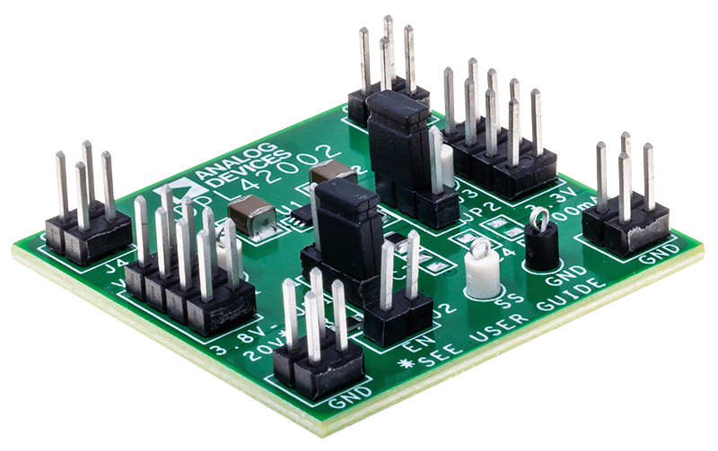
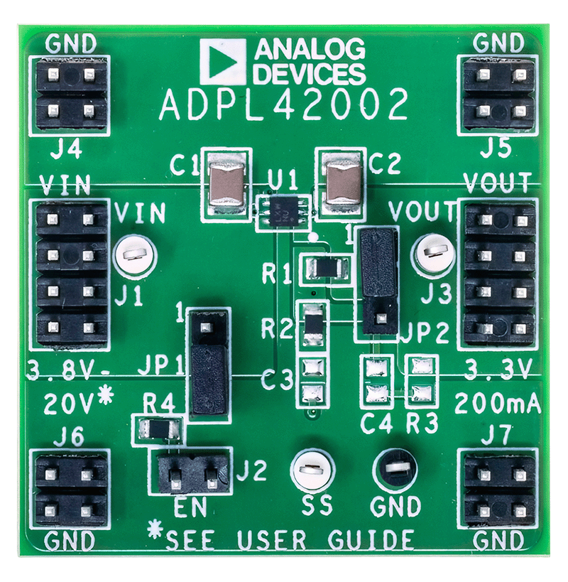
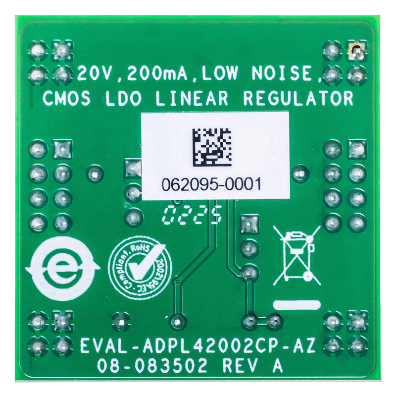
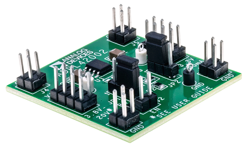
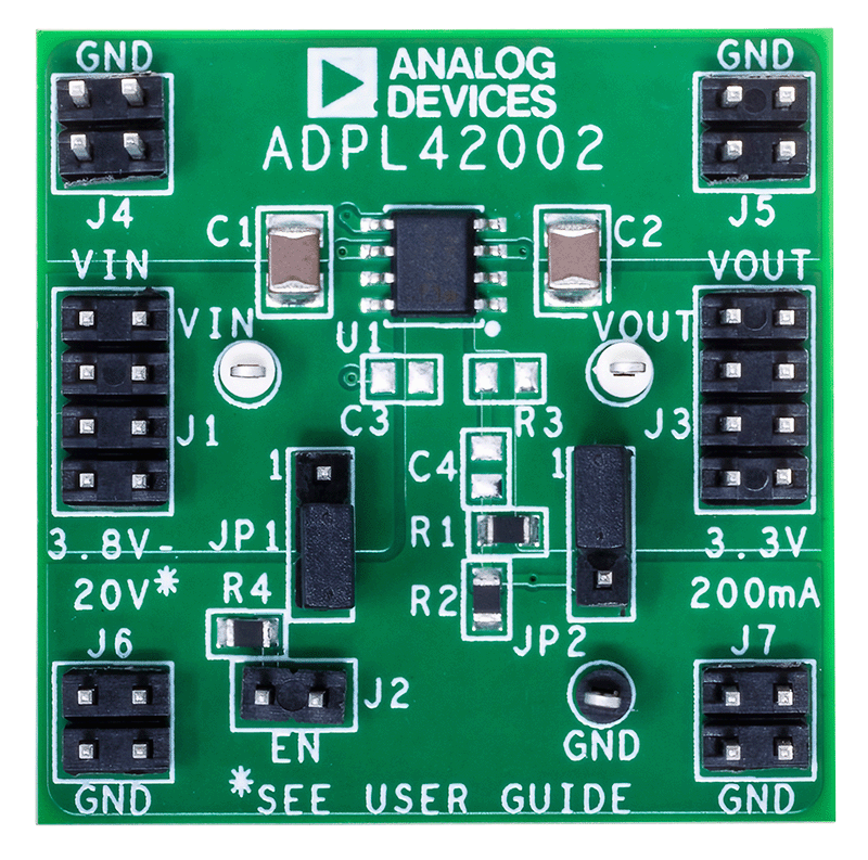
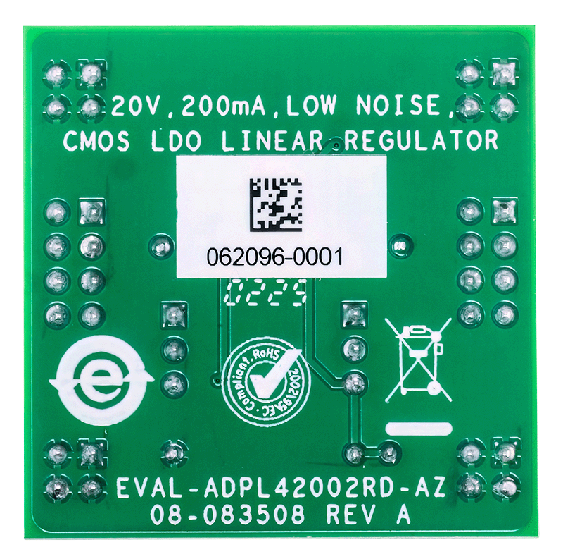
Evaluation Kit for ADPL42002
資料
最新のディスカッション
adpl42002に関するディスカッションはまだありません。意見を投稿しますか?
EngineerZone®でディスカッションを始める