CN0285


Overview
Design Resources
Design & Integration File
- Schematic
- Bill of Materials
- Gerber Files
- PADS Files
- Assembly Drawing
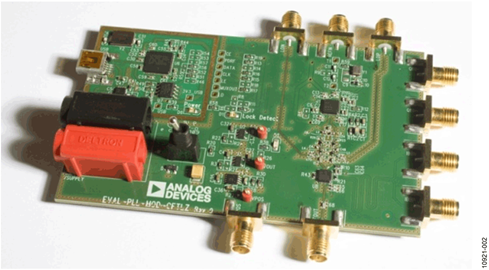
Evaluation Hardware
Part Numbers with "Z" indicate RoHS Compliance. Boards checked are needed to evaluate this circuit.
- EVAL-CN0285-EB1Z ($274.24) Broadband Low Error Vector Magnitude EVM Direct Conversion Transmitter
Device Drivers
Software such as C code and/or FPGA code, used to communicate with component's digital interface.
ADF4350 IIO Wideband Synthesizer GitHub Linux Driver Source Code
Features & Benefits
- Broadband direct conversion transmitter
- 500MHz to 4.4GHz RF
- Low phase noise
- Low error vector magnitude (EVM)
Product Categories
Markets and Technologies
Parts Used
Documentation & Resources
-
UG-521: Evaluating the CN-0285 Wideband Tx Modulator Solution3/7/2013PDF240 kB
Circuit Function & Benefits
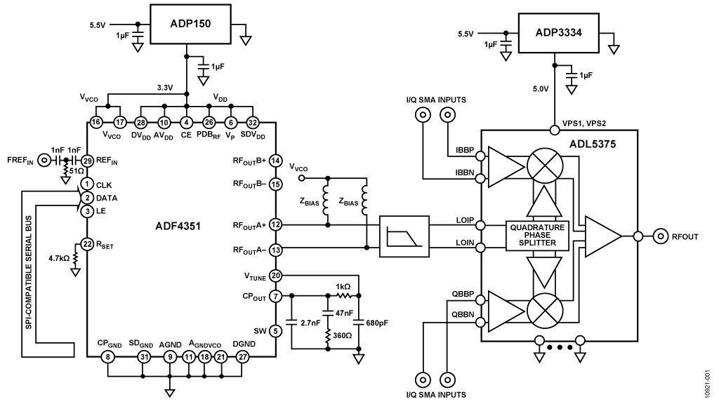
This circuit is a complete implementation of the analog portion of a broadband direct conversion transmitter (analog baseband in, RF out). RF frequencies from 500 MHz to 4.4 GHz are supported using a phase-locked loop (PLL) with a broadband, integrated voltage controlled oscillator (VCO). Harmonic filtering of the local oscillator (LO) from the PLL ensures excellent quadrature accuracy, sideband suppression, and low EVM.


Low noise, low dropout regulators (LDOs) ensure that the power management scheme has no adverse impact on phase noise and EVM. This combination of components represents industry leading direct conversion transmitter performance over a frequency range of 500 MHz to 4.4 GHz.
Circuit Description
The circuit shown in Figure 1 uses the ADF4351, a fully integrated fractional-N PLL IC, and the ADL5375 wideband transmit modulator. The ADF4351 provides the LO signal for the ADL5375 transmit quadrature modulator, which upconverts analog I/Q signals to RF. Taken together, the two devices provide a wideband, baseband IQ-to-RF transmit solution. The ADF4351 is powered off the ultralow noise 3.3 V ADP150 regulator for optimal LO phase noise performance. The ADL5375 is powered off a 5 V ADP3334 LDO. The ADP150 LDO has an output voltage noise of only 9 μV rms and helps to optimize VCO phase noise and reduce the impact of VCO pushing (equivalent to power supply rejection).
Filtering is required on the ADF4351 RF outputs to attenuate harmonic levels to minimize errors in the quadrature generation block of the ADL5375. From measurement and simulation, the odd-order harmonics contribute more than even-order harmonics to quadrature error and, if attenuated to below −30 dBc, results in sideband suppression performance of −40 dBc or better. The second harmonic (2H) and third harmonic (3H) levels of the ADF4351 are as given in the data sheet and shown in Table 1.
To get the third harmonic below −30 dBc, approximately 20 dB of attenuation is required.
| Harmonic Content | Value (dBc) | Description |
| Second | -19 | Fundamental VCO output |
| Third | -13 | Fundamental VCO output |
| Second | -20 | Divided VCO output |
| Third | -10 | Divided VCO output |
This circuit gives four different filter options to cover four different bands. The filters were designed with a 100 Ω differential input (ADF4351 RF outputs with appropriate matching) and a 50 Ω differential output (ADL5375 LOIN differential impedance). A Chebyshev response was used for optimal filter roll-off at the expense of increased pass-band ripple.
The filter schematic is shown in Figure 3. This topology allows the use of either a fully differential filter to minimize component count, a single-ended filter for each output, or a combination of the two. It was determined that for higher frequencies (>2 GHz) two single-ended filters gave the best performance because the series inductor values are twice the value compared to a fully differential filter and, hence, the impact of component parasitics is reduced. For lower frequencies (<2 GHz), a fully differential filter provides adequate results.
The ADF4351 output match consists of the ZBIAS pull-up and, to a lesser extent, the decoupling capacitors on the supply node. To get a broadband match, it is recommended to use either a resistive load (ZBIAS = 50 Ω) or a resistive in parallel with a reactive load for ZBIAS. The latter gives slightly higher output power, depending on the inductor chosen. Note that it is possible to place the parallel resistor as a differential component (that is, 100 Ω) in Position C1c to minimize board space (see Filter Type B, Table 2).
Design the filter with a cutoff approximately 1.2 times to 1.5 times the highest frequency in the band of interest. This cutoff allows margin in the design, because typically the cutoff is lower than designed due to parasitics. The effect of printed circuit board (PCB) parasitics can be simulated in an electromagnetic (EM) simulation tool for improved accuracy.

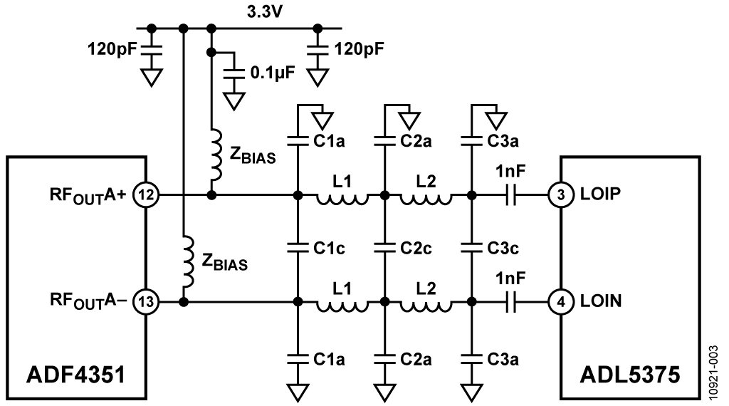
| Frequency Range (MHz) | ZBIAS | L1 (nH) | L2 (nH) | C1a (pF) | C1c (pF) | C2a (pF) | C2c (pF) | C3a (pF) | C3c (pF) |
| 500 to 1300 (Filter Type A) | 27 nH||50Ω | 3.9 | 3.9 | DNI | 4.7 | DNI | 5.6 | DNI | 3.3 |
| 850 to 2450 (Filter Type B) | 19 nH||(100Ω in Position C1c) | 2.7 | 2.7 | 3.3 | 100Ω | 4.7 | DNI | 3.3 | DNI |
| 1250 to 2800 (Filter Type C) | 50Ω | 0Ω | 3.6 | DNI | DNI | 2.2 | DNI | 1.5 | DNI |
| 2800 to 4400 (Filter Type D) | 3.9 nH | 0Ω | 0Ω | DNI | DNI | DNI | DNI | DNI | DNI |
As can be seen from Table 2, at frequencies lower than 1250 MHz, a fifth-order filter is required. For 1.25 GHz to2.8 GHz, third-order filtering is sufficient. For frequencies more than 2.8 GHz, filtering is not required because the harmonic levels are sufficiently low to meet the sideband suppression specifications.

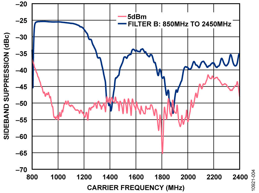

A sweep of sideband suppression vs. frequency is shown in Figure 4 for the circuit using Filter Type B (800 MHz to 2400 MHz). In this sweep, the test conditions were the following:
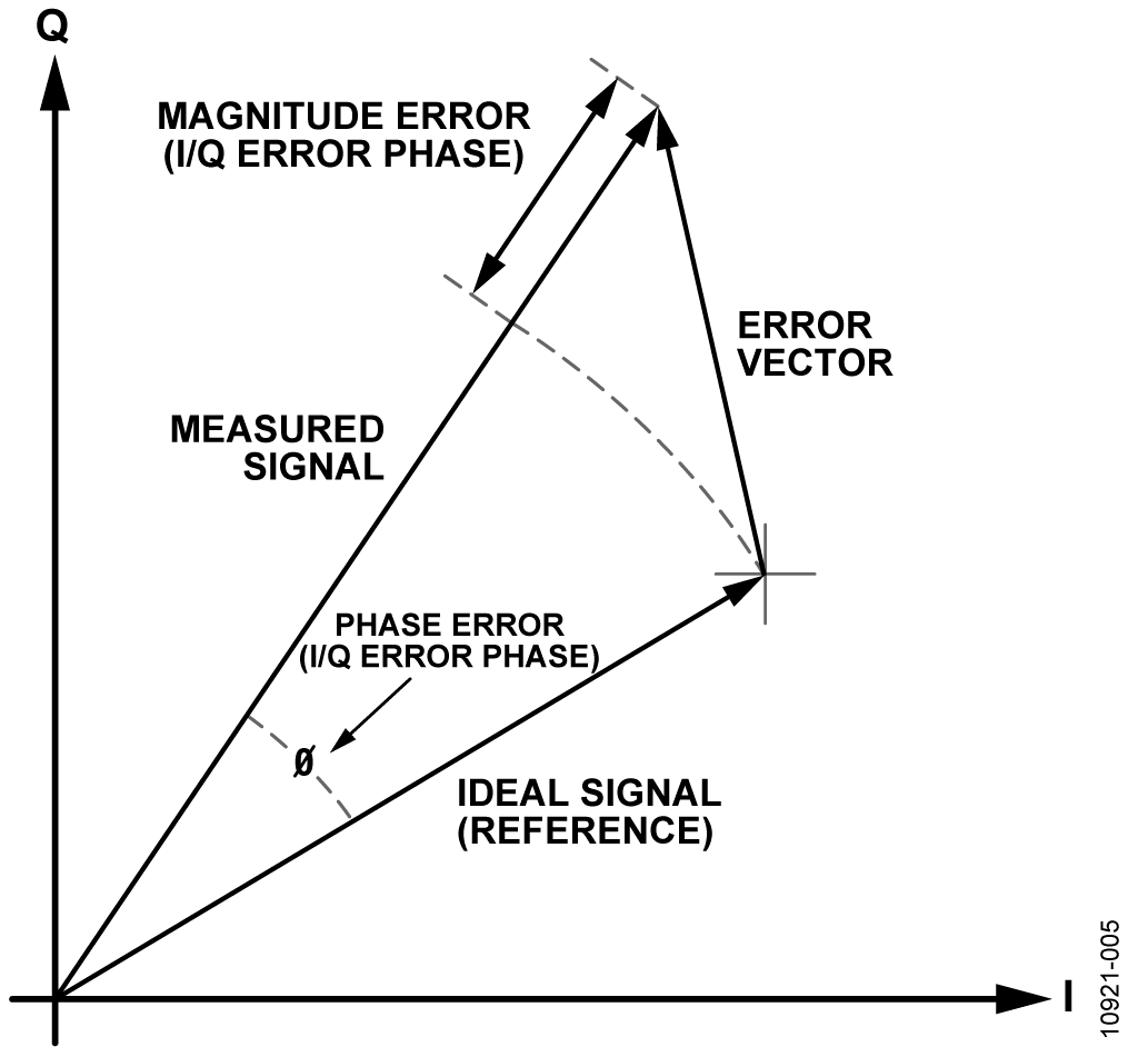
Baseband I/Q amplitude = 1 V p-p differential sine waves in quadrature with a 500 mV (ADL5375-05) dc bias Baseband I/Q frequency (fBB) = 1 MHz. EVM is a measure of the quality of the performance of a digital transmitter or receiver and is a measure of the deviation of the actual constellation points from their ideal locations, due to both magnitude and phase errors (see Figure 5).
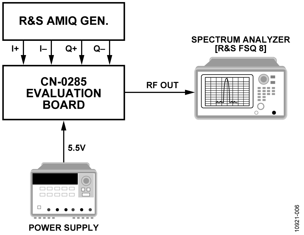
EVM measurements are given in Table 3 comparing the results with and without the filter. In this case, the baseband I/Q signals were generated using 3GPP Test Model 4 using a Rohde & Schwarz AMIQ I/Q modulation generator with differential I and Q analog outputs. Filter Type B was also used. A block diagram of the test setup for the EVM is shown in Figure 6. For comparative purposes, the ADF4350 is also measured. Lower EVM due to in-band PLL noise improvements on the ADF4351 can be seen in Table 3. Other contributing factors to the EVM improvement are the lower phase frequency detector (PFD) spurious levels on the ADF4351.
| Frequency (MHz) | ADF4350 Composite EVM No LO Filtering | ADF4350 Composite EVM with LO Filtering, Filter B | ADF4351 Composite EVM with LO Filtering, Filter B |
| 2140 | 3.27% | 1.31% | 1.02% |
| 1800 | 1.46% | 1.13% | 0.95% |
| 900 | 10.01% | 1.03% | 1.96% |

In addition to the improvement in sideband suppression and EVM, there is also a performance benefit to driving the ADL5375 LO inputs differentially. This benefit improves modulator output IP2 performance by 2 dB to 5 dB, compared with single-ended LO drive. Note that most external VCOs only come with a singleended output, so using the differential outputs on the ADF4351 provides a benefit over an external VCO in this case.
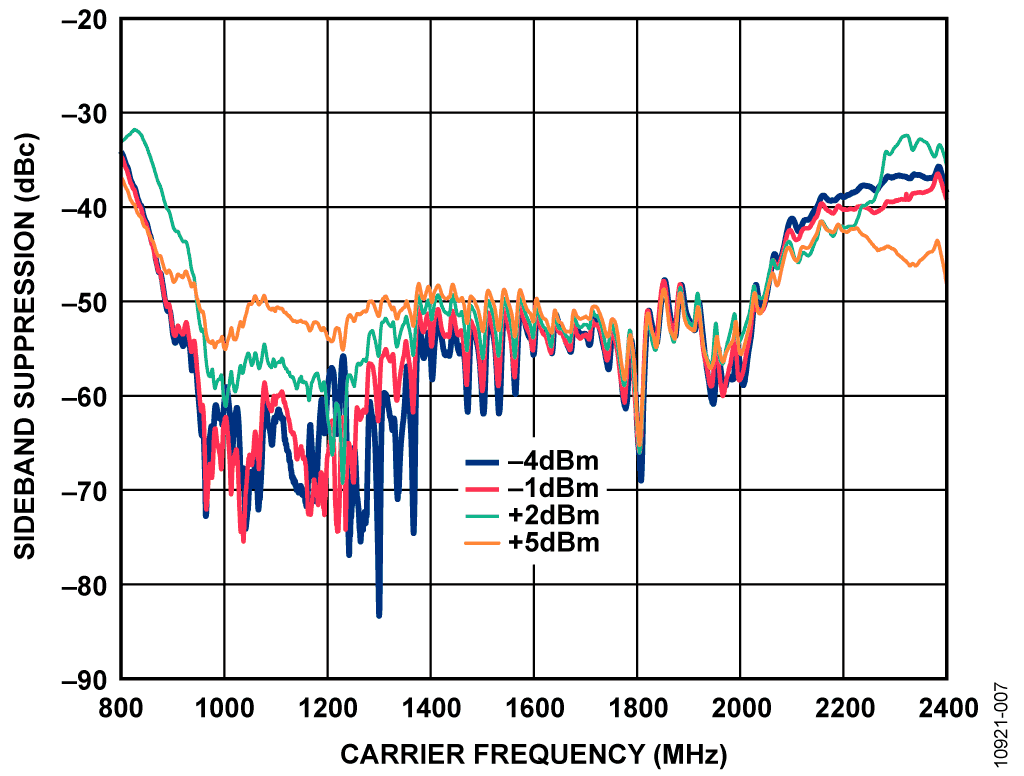
Figure 7 shows sideband suppression results using an 850 MHz to 2450 MHz filter (Filter Type B).

A complete design support package for this circuit note can be found at http://www.analog.com/CN0285-DesignSupport.
Common Variations
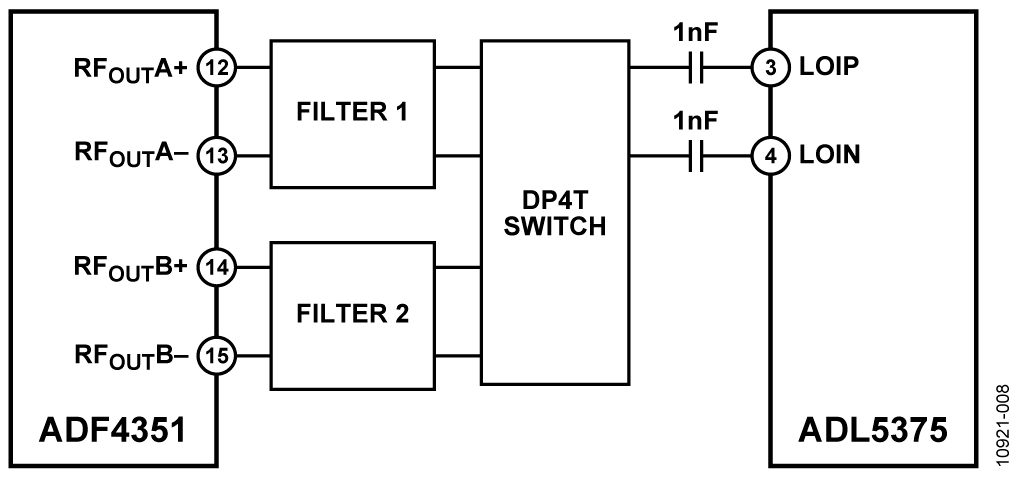
It is possible to use the auxiliary outputs on the ADF4351 to switch between two filter types where wideband operation beyond that possible with one single filter is required (see Figure 8). An RF double-pole, 4-throw switch (DP4T) is used to select the differential outputs of either Filter 1 or Filter 2.

Circuit Evaluation & Test
The EVAL-CN0285-EB1Z evaluation board contains the circuit described in CN-0285, allowing for the quick setup and evaluation of the performance of the circuit. The control software for the EVAL-CN0285-EB1Z uses the standard ADF4351 programming software located on the CD that accompanies the evaluation board.
Equipment Needed
The following equipment is needed:
- A standard PC running Windows® XP, Windows Vista (32- bit), or Windows 7 with a USB port
- The EVAL-CN0285-EB1Z circuit evaluation board
- The ADF435x programming software
- 5.5 V power supplies
- An I-Q signal source, such as the Rohde & Schwarz AMIQ
- A spectrum analyzer, such as the Rohde & Schwarz FSQ8
For additional details, see the UG-521 User Guide, the ADF4351 data sheet, and the ADL5375 data sheet.
Getting Started
See the UG-521 User Guide, for software installation and test setup. The user guide also includes the block diagram, the application schematic, the bill of materials, and the layout and assembly information. In addition, see the ADF4351 data sheet and the ADL5375 data sheet for additional details.
Functional Block Diagram
See Figure 1 and Figure 6 in this document, and also see the UG-521 User Guide.
Setup and Test
After setting up the equipment, use standard RF test methods to measure the sideband suppression of the circuit.