AN-1364: Differential Filter Design for a Receive Chain in Communication Systems
Introduction
RF engineers often see single-ended 50 Ω systems in design. Some of them feel that the differential circuit is not easy to design, test, and debug. Meanwhile, for better performance the differential system is often applied in communication systems especially in the IF stage. Among those difficulties, a differential filter is a key concern. This application note looks at some basic filter key specifications concepts, a few types of frequently used filter responses, a Chebyshev Type 1 filter application, and step-by-step instructions on how to transfer a single-ended filter design to a differential filter design. A differential filter design example is in this application note as well as a few points on how to optimize differential circuit PCB design.
Differential Circuit Advantages
This section discusses differential circuit advantages in RF signal chain applications compare to single-ended circuits.
The user can reach a higher signal amplitude with a differential circuit than with a single-ended circuit. With the same power supply voltage, a differential signal can provide double the amplitude compared to a single-ended signal; it provides better linearity performance and SNR performance.


Differential circuits are fairly immune to outside EMI and crosstalk from nearby signals. This is because the received voltage is doubled, and theoretically, the noise affects the tightly coupled traces equally. Therefore, they cancel each other out.
Differential signals also tend to produce less EMI. This is because the changes in signal levels (dV/dt or dI/dt) create opposing magnetic fields, again canceling each other out.
Differential signals can reject even order harmonics. For example, use continuous wave (CW) passes through one gain stage.
If using one single-ended amplifier, the output can be expressed as shown in Figure 2, Equation 1, and Equation 2.
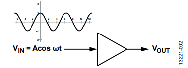
Figure 2. Single-Ended Amplifier

where … indicates that the sequence continues.
If using one differential amplifier, the input and output are shown in Figure 3, Equation 3, Equation 4, Equation 5, and Equation 6.


where … indicates that the sequence continues.
Ideally, the output does not have any even order harmonics.
Therefore, in the communication system, for better performance consideration, a differential circuit is preferred.
Filters
Filter Specification
Cutoff frequency, corner frequency, or break frequency is a boundary in a system's frequency response at which energy flowing through the system begins to reduce (attenuate or reflect) rather than passing through.


In-band ripple is the fluctuation of insertion loss within the pass band.


Phase linearity is the direct proportionality of phase shift to frequency over the frequency range of interest.


Group delay is a measure of the time delay of the amplitude envelopes of the various sinusoidal components of a signal through a device under test, and is a function of frequency for each component.


Filter Comparison
| Filter | S21 Response | Pros | Cons |
| Butterworth | See Figure 8 | Very good flatness in pass band | Rolls off slowly in stop band |
| Elliptic | See Figure 9 | Rolls off very quickly in close in stop band | Has equalized ripple in both pass band and stop band, this affects the stop band rejection performance |
| Bessel | See Figure 10 | Maximum flat group/phase delay | Very slow roll off in stop band |
| Chebyshev Type I | See Figure 11 | Rolls off quickly in stop band; no equalized ripple in stop band | Has equalized ripple in pass band |
| Chebyshev Type II | See Figure 12 | No ripple in pass band | Roll off is not very fast; has equalized ripple in stop band |


The IF filter designed in the communication receive chain is basically a low-pass filter or band-pass filter; it is used for rejecting the aliasing signals together with spurs generated by active components. The spurs include functions such as harmonics and IMD products. With the filter, the receive chain can provide clean and good SNR signals for ADC to analyze.
The Chebyshev Type I filter was chosen as the topology because it has good in-band flatness, quick roll off in stop band, and no equiripple in stop band.
Designing a Low-Pass Filter
Because the receive IF filter is used to reject spurs and aliasing signals, using a faster stop band roll-off is better; however, faster roll-off means higher-order components. Nevertheless, a high-order filter is not recommended because following reasons:
- Difficulty for tuning at the design and debug stage.
- Difficulty in mass production, because capacitors and inductors have part-to-part variation; it is difficult for filters on each PCB board to have the same response.
- Large PCB size.
In general, use a seventh-order or lower filter. Meanwhile, with the same order components, if bigger in-band ripple isn’t a problem, faster roll-off in stop band is a payout.
Define the response needed by specifying the required attenuation at a selected frequency point.
To determine the maximum amount of ripple in the pass band, keep the specification to the maximum limit of the system requirement, this can help get faster roll-off in stop band.
Use low-cost filter software, such as MathCad®, MATLAB®, or ADS to design the single-ended low-pass filter.
Alternatively, design the filter by manually. RF Circuit Design by Chris Bowick (see the References section) offers a useful guide.
To determine the orders of the filter, normalize the frequency of interest by dividing it with the cutoff frequency of the filter.

For example, if the in-band ripple needs to be 0.1 dB, the 3 dB cutoff frequency is 100 MHz. At 250 MHz the rejection needs to be 28 dB, the frequency ratio is 2.5. A third-order low-pass filter can meet this requirement. If the source impedance of the filter is 200 Ω, the load impedance of the filter is also 200 Ω, RS/RL is 1; use a capacitor as the first component. Then the user receives a normalized C1 = 1.433, L2 = 1.594, C3 = 1.433, if the fc is 100 MHz, use Equation 7 and Equation 8 to finalized results:

where:
CSCALED is the final capacitor value.
LSCALED is the final inductor value.
Cn is a low-pass prototype element value.
Ln is a low-pass prototype element value.
RL is the final load resistor value.
fc is the final cutoff frequency.
C1SCALED = 1.433/(2π × 100 × 106 × 200) = 11.4 pF
L2SCALED = (1.594 × 200)/(2π × 100 × 106) = 507.4 nH
C3SCALED = 11.4 pF
The circuit is shown in Figure 13.


Convert the single-ended filter into a differential filter (see Figure 14).


Using the real world value for each component, the filter is updated as shown in Figure 15.


Note that if the output impedance of the mixer or IF amplifier and the input impedance of ADC are capacitive, it is better to consider using a capacitor as the first component and a capacitor as the last component. Also, it is important to tune the first capacitor and last stage capacitor value at a higher rate (at least 0.5 pF) than the capacitance of the output impedance of the mixer or IF amplifier and input impedance of ADC. Otherwise, it is very difficult to tune the filter response.
Designing a Band-Pass Filter
In communication systems when the IF frequency is quite high, some low frequency spurs also need to be filtered out, like half IF spur. For this kind of application, design a band-pass filter. For a band-pass filter, it is not necessary to be symmetrical for low frequency rejection and high frequency rejection. The easy way to design a band-pass antialiasing filter is to design a low-pass filter first, then add one shunt inductor in parallel with the shunt capacitor at the final stage of the filter to limit low frequency components (a shunt inductor is a high-pass resonance pole). If one stage high-pass inductor is not enough, add one more shunt inductor in parallel with the first stage shunt capacitor to get more rejection for low frequency spurs. After adding the shunt inductor, tune all components again, to receive the right out of band rejection specification and then finalize the filter components value.
Note that in general for a band-pass filter, serial capacitors are not recommended because they increase tuning and debugging difficulty. The capacitance value is usually quite small, it is heavily affected by parasitic capacitance.
Application Example
This section describes an application example of filter design between the ADL5201 and AD6641. The ADL5201 is a high performance IF digitally controlled gain amplifier (DGA), which is designed for base station real IF receiver applications or digital predistortion (DPD) observation paths; it has a 30 dB gain control range, very high linearity whose OIP3 reaches 50 dBm, and a voltage gain of about 20 dB. The AD6641 is a 250 MHz bandwidth DPD observation receiver that integrates a 12-bit 500 MSPS ADC, a 16,000 × 12 FIFO, and a multimode back end that allows users to retrieve the data through a serial port. This filter example is a DPD application.
Following are some of the band-pass filter design specifications taken from a real communication system design:
- Center frequency: 368.4 MHz
- Bandwidth: 240 MHz
- Input and output impedance: 150 Ω
- In-band ripple: 0.2 dB
- Insertion loss: 1 dB
- Out of band rejection: 30 dB at 614.4 MHz
To build the example design, use the following steps:
- Start with a single-ended, low-pass filter design (see Figure 18).
- Change the single-ended filter into a differential filter. Keep the source and load impedance the same, shunt all capacitors, and cut all serial inductors in half and put them in the other differential path (see Figure 19).
- Optimize the components ideal value with real world value (see Figure 20).
- For subsystem level simulation, add the ADL5201 DGA S-parameter file at the input, use the voltage control voltage source to model the AD6641 ADC at the output of the filter. To change the low-pass filter into a band-pass filter, add two shunt inductors: L7 in parallel with C9 and L8 in parallel with C11. C12 represents the AD6641 input capacitance. R3 and R4 are two load resistors put at the input of AD6641 to be the load of filter. The AD6641 input is high impedance. After tuning, see Figure 21.
- The simulation results with ideal components is shown in Figure 16.


- Replace all ideal inductors with the inductor S-parameter files of the intended device (for example, Murata LQW18A). The insertion loss is a little bit higher than using ideal inductors. The simulation result changes slightly as shown in Figure 17.


Differential Filter Layout Consideration
The differential traces in a pair need to be of an equal length. This rule originated from the fact that a differential receiver detects where the negative and positive signals cross each other at the same time—the crossover point. Therefore, the signals arrive at the receiver at the same time for proper operation.
The traces within a differential pair need to be routed close to each other, the coupling between the neighboring lines within a pair is small if the distance between them is >2× the dielectrical thickness. Also, this rule is based upon the fact that because the differential signals are equal and opposite, and if external noise equally interferes with these signals, the noise nullifies. Similarly, any unwanted noise induced by the differential signals into adjacent conductors cancels each other out if traces are routed side by side.
The trace separation within a differential pair needs to be constant over its entire length. If the differential traces are routed close together, then they impact the overall impedance. If this separation is not maintained from the driver to the receiver, there are impedance mismatches along the way, resulting in reflections.
Use a wide pair-to-pair spacing to minimize crosstalk between pairs.
If using copper fill on the same layer, increase the clearance from the differential traces to the copper fill. A minimum clearance of 3× the trace width from the trace to the copper fill is recommended.
Reduce intra pair skew in a differential pair by introducing small meandering corrections close to the source of the skew (see Figure 22).


Avoid tight (90°) bends when routing differential pairs (see Figure 23).


Using symmetric routing when routing differential pairs (see Figure 25).
If test points are required, avoid introducing trace stubs and place the test points symmetrically (see Figure 24).


Consider relaxing the filter component value tuning workloads on the printed circuit board (PCB); it is important to keep the parasitic capacitance and inductance as low as possible. The parasitic inductance may not be significant compared to the design value of the inductor in the filter design. The parasitic capacitance is more critical for a differential IF filter. The capacitors in the IF filter designs are only a few picofarads, if the parasitic capacitance reaches a few tenths of picofarads, it affects the filter response significantly. To avoid parasitic capacitance, it is good practice to avoid any ground or power planes under the differential routing region and under power supply chokes.
One example of the differential filter PCB layout is Analog Devices, Inc., receiver reference design board (see Figure 26). Figure 26 shows a fifth-order filter between the ADL5201 and the AD6649. The AD6649 is 14-bit 250 MHz pipeline ADC that has very good SNR performance.


References
Bowick, Chris. RF Circuit Design. Newnes. 1997.
Calvo, Carlos. “The Differential-Signal Advantage for Communications System Design.” Analog Devices, Inc.