CN0548


Overview
Design Resources
Design & Integration File
- Schematic
- Bill of Materials
- Gerber Files
- Assembly Drawing
- Layout Files
Evaluation Hardware
Part Numbers with "Z" indicate RoHS Compliance. Boards checked are needed to evaluate this circuit.
- EVAL-ADICUP3029 ($52.97) Ultralow Power Cortex-M3 Arduino Form Factor Compatible Development Board
- EVAL-CN0548-ARDZ ($95.23) Isolated, High Voltage and Current Measurement Board
Device Drivers
Software such as C code and/or FPGA code, used to communicate with component's digital interface.
Features & Benefits
- Wide Current (+/-10 A) and Voltage (80 V) Input Range
- Configurable gain/attenuation settings
- Galvanically Isolated
- Arduino form factor compatible
Markets and Technologies
Parts Used
Documentation & Resources
-
CN0548 User Guide1/25/2022WIKI
-
Solutions For Rapid Prototyping: Answering the Needs of Practicing Engineers8/23/2023PDF784 K

Circuit Function & Benefits
Testing and evaluating power systems in industrial and communications settings often requires multiple voltage and current measurements. Individual supplies may be referenced to different grounds, have either positive or negative polarity, or may be floating with no defined relationship to other power domains. Such scenarios necessitate either individual floating multimeters, or multichannel meters with per-channel isolation, which are physically cumbersome and expensive.


The circuit shown in Figure 1 is a complete, isolated current and voltage measurement system for industrial, telecommunications, instrumentation, and automated test equipment (ATE) applications. The system is galvanically isolated and will tolerate up to +/-250 V between the host controller and measurement grounds. The isolation design includes both digital data and power domain signals; no additional power source is required from the circuit being measured.
The current input range is +/-10 A and the voltage input range is selectable from 16 V to 80 V, with several ranges between these values. Both voltage and current inputs feature 16-bit resolution with adjustable output data rate and signal bandwidth, including modes that reject both 50 Hz and 60 Hz line noise.
The circuit is compatible with Arduino form-factor platform boards, and supports logic voltages from 1.8 V to 5 V. When paired with the open-source firmware example, application software can easily communicate with the reference design over the Linux Industrial Input/Output (IIO) framework using the libiio library, which includes bindings for C, C#, MATLAB, Python, and LabVIEW.
Circuit Description
Voltage and Current Measurement Connections
The CN0548 can be configured to accommodate a variety of measurement situations. The current sense input can be referenced to either the positive or negative voltage input terminal or any voltage in between, and measurement ground is isolated from the development platform and the connected host computer’s ground.
Figure 2 shows the connections for measuring a circuit with a grounded 15 V supply and grounded load. Load current is measured at the high side of the load.

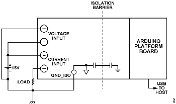
Figure 3 shows the connections for measuring load current at the low side (ground return) of the load.


Figure 4 shows the connections for measuring a -48 V supply, with current measured at the load's ground return.

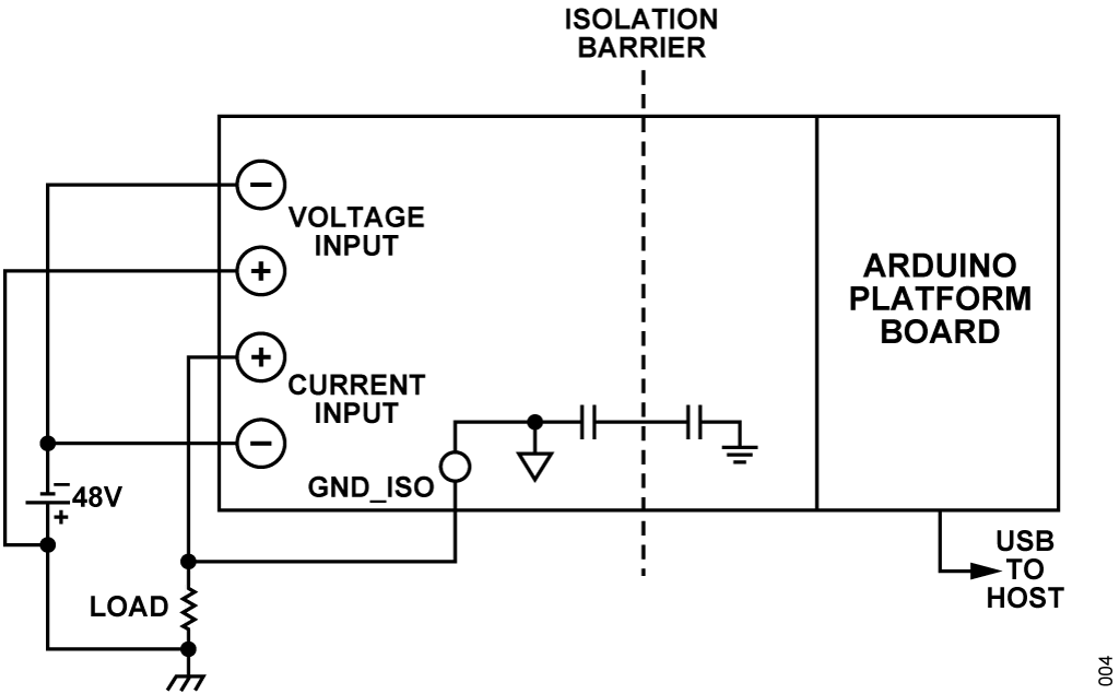
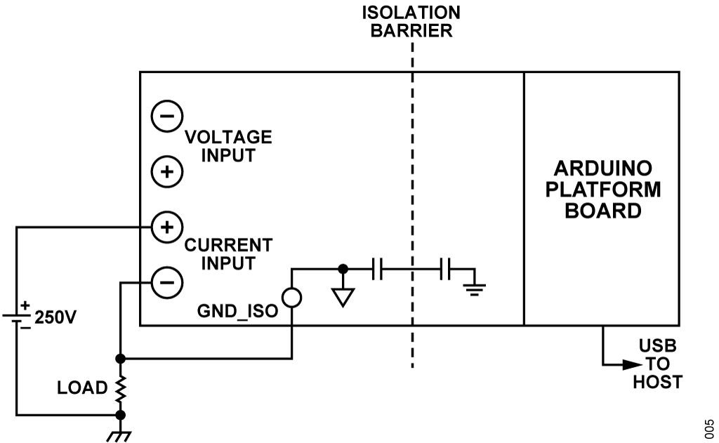
Figure 5 shows the connections for a high-side current measurement, with a supply voltage as high as 250 V. While the voltage measurement channel can tolerate voltages up to +/-250 V at its inputs without damage, the output will be saturated and will not produce a valid measurement.

Voltage Input
An LT1997-2 precision, high voltage funnel amplifier with internal matched resistor network scales the input voltage to within the input range of the ADC. This device has a gain error of 0.006% and a gain drift of 1 ppm/°C. Thirty eight unique attenuation factors can be selected by pin-strapping the +INA , +INB, +INC, -INA, -INB, and -INC inputs, implemented via jumpers on the CN0548.


Table 1 lists five jumper settings that cover most applications as well as the allowable input voltage for the circuit. Refer to the LT1997-2 data sheet for a comprehensive list of attenuation factors. Note that the gain setting jumpers should be configured before connecting the CN0548 to a live circuit, and do not move jumpers when connected to a live circuit.
| Input Range | Attenuation | +INA | +INB | +INC | -INA | -INB | -INC |
| 80V | 20 | OPEN | -VIN | +VIN | OPEN | +VIN | -VIN |
| 40V | 10 | +VIN | OPEN | OPEN | -VIN | OPEN | OPEN |
| 27V | 6.67 | -VIN | OPEN | +VIN | +VIN | OPEN | -VIN |
| 20V | 5 | OPEN | +VIN | OPEN | OPEN | -VIN | OPEN |
| 16V | 4 | OPEN | OPEN | +VIN | OPEN | OPEN | -VIN |
The CN0548 voltage input can be set to unipolar or bipolar input range by configuring the LT1997-2 REF pin and AD7798 AIN3- pin voltages as shown in Table 2.
| Measurement Mode | LT1997-2 REF | AD7798 AIN3- | Input Range (80V span) |
| Unipolar | GND | GND | 0 V to 80 V |
| Bipolar | 2.048 V | 2.048 V | -40 V to +40 V |
Current Input
The AD8418A is a bidirectional, high voltage, zero-drift current sense amplifier. It features fixed gain of 20 V/V, with a 10 kHz bandwidth with a maximum ±0.15% gain error over its entire operating temperature range. The amplifier's output voltage directly interfaces to channel 1, AIN1- and AIN1+ of the ADC. The AD8418A offers excellent input common-mode rejection from -2 V to +70 V.


As shown in Table 3, the AD8418A performs bidirectional current measurements across a 10 mΩ, 2 W current sense resistor between the ISENSE input terminals. The maximum input current is+/-10 A in bipolar mode. The unipolar input range is 0 A to as high as 14 A, limited by the power dissipation of the sense resistor. The AD8418A output requires 32 mV of headroom to GND; refer to Unipolar and Bipolar Current Measurement Test Results.
| Measurement Mode | AD8418A REF | AD7798 AIN1- | Input Range |
| Unidirectional | GND | GND | 0 V to 14 A |
| Bidirectional | 2.048 V | 2.048 V | -10 V to +10 A |
Analog to Digital Conversion
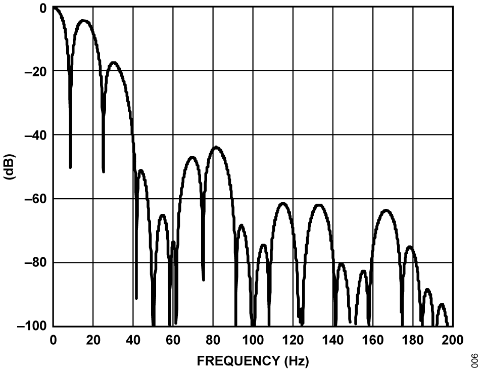
The AD7798 is a 16-bit low power, high-precision Σ-Δ analog to digital converter (ADC) intended for the measurement of wide dynamic range, low frequency signals, such as those in pressure transducers, weigh scales, and precision measurement applications. The AD7798 has three buffered differential inputs with a programmable instrumentation amplifier (in-amp), and on-chip digital filtering. An external reference voltage between 100 mV and 5.25 V determines the full-scale input range. The output data rate of the AD7798 is user-programmable from 4.17 to 470 sps; the measurement bandwidth, and hence sensitivity to noise, is proportional to the output data rate. Most power supply measurement applications do not require a high sample rate and can take advantage of the narrow bandwidth provided by lower output data rate modes. Furthermore, sample rates of 16.7 sps and lower provide simultaneous rejection of 50 Hz and 60 Hz line noise. The AD7798 uses slightly different filter types, depending on the output data rate, in order to minimize the effect of internal noise sources. Figure 8 shows the filter response for the for the 16.7 Hz mode. Refer to the AD7798 data sheet for a complete detailed description of all filter modes.

The analog inputs to the AD7798 are fully differential, with an input range of
The absolute voltage can extend to either supply rail when the inputs are in unbuffered mode and the in-amp is inactive, which is the configuration that the CN0548 uses by default.
The CN0548 presents high-level, buffered signals to the AD7798, so the gain can be set to 1 and buffers disabled, maximizing the input range. The 4.096 V reference voltage results in a +/-4.096 V input range, and readings are valid even when the ADC inputs are at or slightly below ground.
Reference Voltages
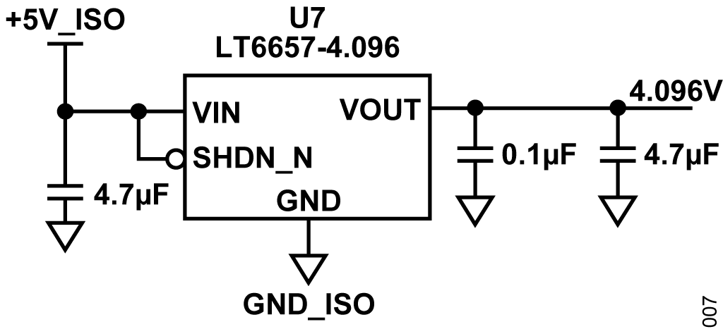
There are two voltage references used on the CN0548 board. An A-grade LT6657, shown in Figure 9, provides a 4.096 V reference voltage to the AD7798. This part offers exceptionally low noise for a bandgap reference; only 0.5 ppmP-P or an average of 1.24 μVp-p in the 0.1 Hz to 10 Hz bandwidth. It is stable with a large output capacitor, which serves to reduce high-frequency noise as well as providing a low-impedance for the AD7798’s dynamic sampling current. The line regulation of the LT6657 for 4.096 V output reference is typically well below 1 ppm/V. Load regulation is also less than 2 μV/mA. A 5 mA change in load current shifts output voltage by only 10 μV.

An LT6656 provides a 2.048 V bias voltage for the VSENSE amplifier, ISENSE amplifier, and ADC negative inputs, allowing the input terminals to accommodate bipolar ranges.
Noise Performance
The highest output noise voltage for the LT1997-2 is at attenuation of 4, which is about 1 μVp-p. The LT6657 has about 2 μVp-p output noise. The total (root-sum-square) value of 1 μVp-p and 2.0 μVp-p, or 1.7 μVp-p. The AD7798 quantization noise is 62.5μV, and will thus be the dominant noise source for voltage measurements. The input-referred noise will be approximately 1.2 mV in the 80 V input range.
For the current measurement mode, the AD8418A has an input noise voltage of 2.3 μVp-p from 0.1 Hz to 10 Hz. With a gain of 20, the reflected noise to the output results in 20 × 2.3 μVp-p, or 46 μVp-p. This is still slightly lower than the AD7798 quantization noise. While several codes of flicker are to be expected for a fixed, noiseless input, the AD7798 can still be considered the dominant noise source.
Power and SPI Isolation
A 5 V, serial peripheral interface (SPI) version of the LTM2886 μModule provides isolated +/-5 V power and isolated SPI communication. No external components are required, decoupling capacitors are incorporated into the module. The LTM2886 is extremely tolerant of common mode transients between ground planes; error-free operation is maintained through common mode events greater than 30 kV/us. The LTM2886 includes a separate logic supply pin, allowing the host side logic level to be any voltage between 1.62 V and 5.5 V.
Circuit Board Isolation
Figure 10 and Figure 11 show the circuit board isolation barrier. The board was designed for maximum creepage between grounds, with two 250 V safety rated type Y2 capacitors in series for reducing conducted noise from the LTM2886's internal switching regulator.


Common Variations
For a higher resolution ADC, the AD7799, a 24-Bit, Σ-Δ ADC can be used as an alternative. If a 2.5 V reference is required for the AD7798/AD7799, the ADR381 or ADR391 low noise, low power references are recommended.
For lower full-scale current applications, the AD8417 is bidirectional, zero Drift, current sense amplifier with a gain of 60 V/V.
In an application that requires both signal input attenuation and amplification, the LT1997-3 is an alternative amplifier. The LT1997-3 combines a precision operational amplifier with highly matched resistors to form a one-chip solution for accurately amplifying voltages. An attenuation up to 0.0714 and a gain up to +14 with accuracy of 0.006% (60ppm) can be achieved using no external components.
The maximum potential difference between the CN0548 grounds is+/-250 V, limited by the 470 pF stitching capacitors. Higher voltage applications require modification or removal of the stitching capacitance; the LTM2886 itself can withstand 2500 VRMS between grounds for 1 minute.
For applications requiring higher voltage at the isolated side, the LTM2883 is an alternative part. The LTM2883 is a complete galvanic 6-channel digital µModule® (micromodule) isolator. The isolated side includes ±12.5 V and 5 V nominal power supplies, each capable of providing more than 20 mA of load current. Each supply maybe adjusted from its nominal value using a single external resistor.
Circuit Evaluation & Test
The EVAL-CN0548-ARDZ was tested using an EVAL-ADICUP3029 ultralow power Cortex-M3 Arduino form factor development board. For complete setup details and additional information on the CN-0548, see the CN0548 User Guide.
Equipment Needed
- EVAL- ADICUP3029
- EVAL-CN0548-ARDZ
- Bench top Variable power supply source (ex. Agilent e3631)
- USB CABLE micro Type B to Type A
- 2 pieces banana to banana jack
- Windows, Linux, or Mac computer with serial terminal and Python 3.6 or newer installed
Getting Started
To setup the EVAL-CN0548-ARDZ and the associated software, use the following steps:
- Connect the EVAL-CN0548-ARDZ on top of the EVAL-ADICUP3029 platform board as shown in Figure 12.
- Connect the EVAL-ADICUP3029 to the PC using the micro USB cable provided.
- From the PC drag and drop the prebuilt .hex file onto the DAPLINK drive. Refer to the user guide for the latest hex file.
- Reset the ADICUP3029 by pressing the 3029_RESET button or by unplugging and re-plugging the USB cable.
- Determine the EVAL-ADICUP3029 COM port through the device manager (Windows) or TTY device file (Linux).
- Open the CN0548_simple_plot.py example Python script. (Refer to user guide for script location.) Follow the prompts for setting up the jumpers and entering in the COM (or tty) port number.
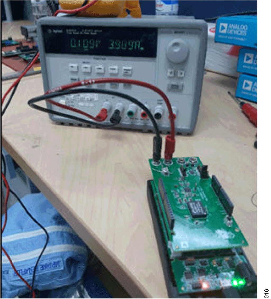
- For voltage sensing measurement, connect the banana connectors at main DC source as shown in Figure 13 and Figure 14. Set the output voltage between 5.99V and 6V and current limit set between 3.9A and 4A.
- For current sensing measurement, connect the banana connectors at main DC source as shown in Figure 17 and Figure 18.


Voltage Measurement Test Setup
The EVAL-CN0548-ARDZ was tested in Unipolar and in Bipolar mode, sweeping the input voltage from 0-40V and -40 to +40V, respectively, in 100 mV steps. The EVAL-CN0548-ARDZ board reading was compared to a Keithley DMM7510 7-1/2 digit multimeter as shown in Figure 13 and Figure 14. The LT1997-2 was set to an attenuation of 20 and the voltage reference for the AD7798 and the LT1997-2 are set to 0V at unipolar and 2.048V at bipolar voltage measurement mode.


Unipolar and Bipolar Voltage Test Results
Figure 15 and Figure 16 show uncorrected output from three individual CN0548 boards. Results are in line with the LT1997-2, LT6657, and AD7798 accuracy specifications. The non-linear "steps" in the transfer function is the point at which the LT1997-2 enters "over-the-top" mode.


Current Measurement Test Setup
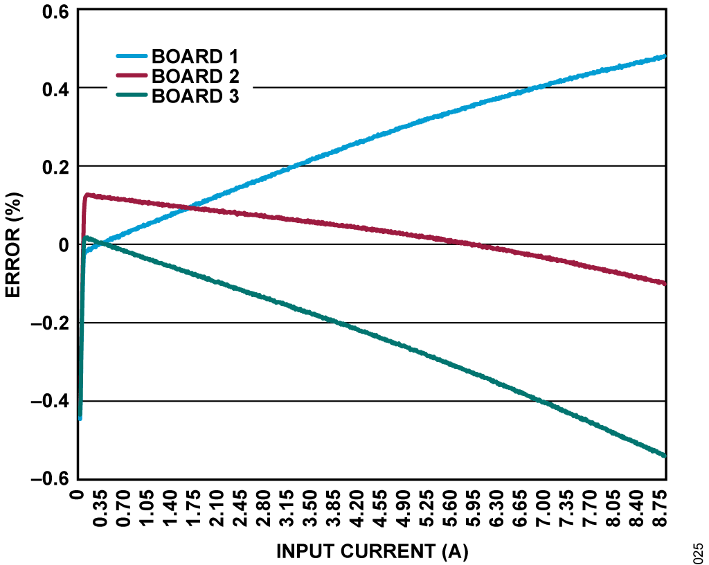
The EVAL-CN0548-ARDZ was tested in Unipolar and in Bipolar mode, sweeping the input current from 0 A to 9 A and -9 A to +9 A, respectively, in 100mA steps. The EVAL-CN0548-ARDZ board reading was compared to a Keithley DMM7510 high-resolution 7½-digit multimeter as seen in Figure 17 and Figure 18.


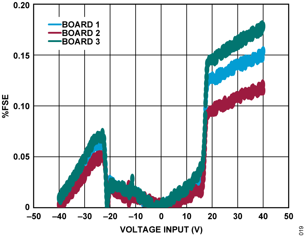
Unipolar and Bipolar Current Measurement Test Results
Figure 19 and Figure 20 show the uncalibrated accuracy of three individual CN0548 boards. The gain error is dominated by the±1% tolerance current sense resistor.