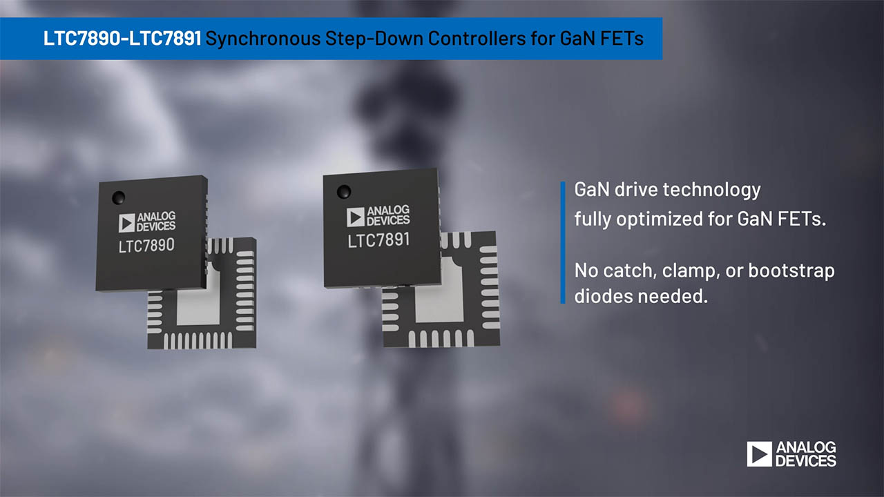
LTC7891
推荐新设计使用用于GaN FET的100 V,低IQ同步降压控制器
- 产品模型
- 2
产品详情
- 为 GaN FET 全面优化的 GDN 驱动器技术
- 宽 VIN 范围:4 V 至 100 V
- 宽输出电压范围:0.8 V ≤ VOUT ≤ 60 V
- 无需环流、箝位或阴极负载二极管
- 内部智能引导开关可防止高端驱动器电源过度充电
- 经过内部优化,智能近零停滞时间或电阻可调停滞时间
- 可调的开/关驱动器强度的分流输出栅极驱动器
- 精确可调驱动器电压和 UVLO
- 低工作 IQ:5 μA(48 VIN 至 5 VOUT)
- 可编程频率(100 kHz 至 3 MHz)
- 可锁相频率(100 kHz 至 3 MHz)
- 展频 (SSFM)
- 28 引脚 (4 mm × 5 mm) 侧面可湿性 QFN 封装
LTC7891是一款高性能、降压DC/DC开关稳压器控制器,通过高达100 V的输入电压驱动所有N通道同步氮化镓(GaN)场效应晶体管(FET)功率级。LTC7891解决了许多使用GaN FET时通常会面临的挑战。与硅金属氧化物半导体场效应晶体管(MOSFET)解决方案相比,LTC7891简化了应用设计,无需保护二极管和其他附加外部组件。
内部智能自举开关可防止BOOST引脚至SW引脚高端驱动器电源在死区时间内过度充电,从而保护顶部GaN FET的栅极。LTC7891在内部优化了两个开关边沿的栅极驱动器时序,以实现智能近零死区时间,从而显著提升效率,甚至在高输入电压下也能实现高频运行。或者,用户可以使用外部电阻调整死区时间以进行裕量调整或定制应用。
LTC7891的栅极驱动电压可在4 V至5.5 V范围内精确调节以优化性能,并且可使用不同的GaN FET,甚至是逻辑电平MOSFET。
请注意,在整篇数据手册中,多功能引脚(如PLLIN/SPREAD)由整个引脚名称或引脚的单个功能表示;例如PLLIN即表示仅与此功能相关。
应用
- 工业电源系统
- 军事航空电子和医疗系统
- 电信电源系统
参考资料
数据手册 1
用户手册 3
视频 5


解决方案设计及宣传手册 1
非常见问题 1
模拟对话 2
ADI 始终高度重视提供符合最高质量和可靠性水平的产品。我们通过将质量和可靠性检查纳入产品和工艺设计的各个范围以及制造过程来实现这一目标。出货产品的“零缺陷”始终是我们的目标。查看我们的质量和可靠性计划和认证以了解更多信息。
| 产品型号 | 引脚/封装图-中文版 | 文档 | CAD 符号,脚注和 3D模型 |
|---|---|---|---|
| LTC7891RUFDM#PBF | 28-Lead QFN (4mm x 5mm, Plastic Side Wettable) | ||
| LTC7891RUFDM#TRPBF | 28-Lead QFN (4mm x 5mm, Plastic Side Wettable) |
这是最新版本的数据手册
软件资源
找不到您所需的软件或驱动?
申请驱动/软件工具及仿真模型
LTspice 2
- LTC7891 Example Circuit – 100V GaN Synchronous Buck Controller with EPC FETs, Input: 15V – 72V, Output: 12V @ 20A, 500kHz Fsw
- LTC7891 - Step-Down (Buck) Regulators
LTspice中提供以下器件型号:
- LTC7891
LTspice®是一款强大高效的免费仿真软件、原理图采集和波形观测器,为改善模拟电路的仿真提供增强功能和模型。
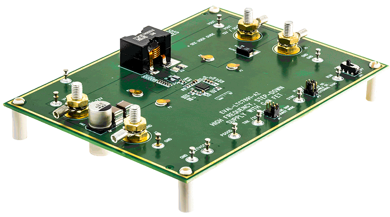
评估套件
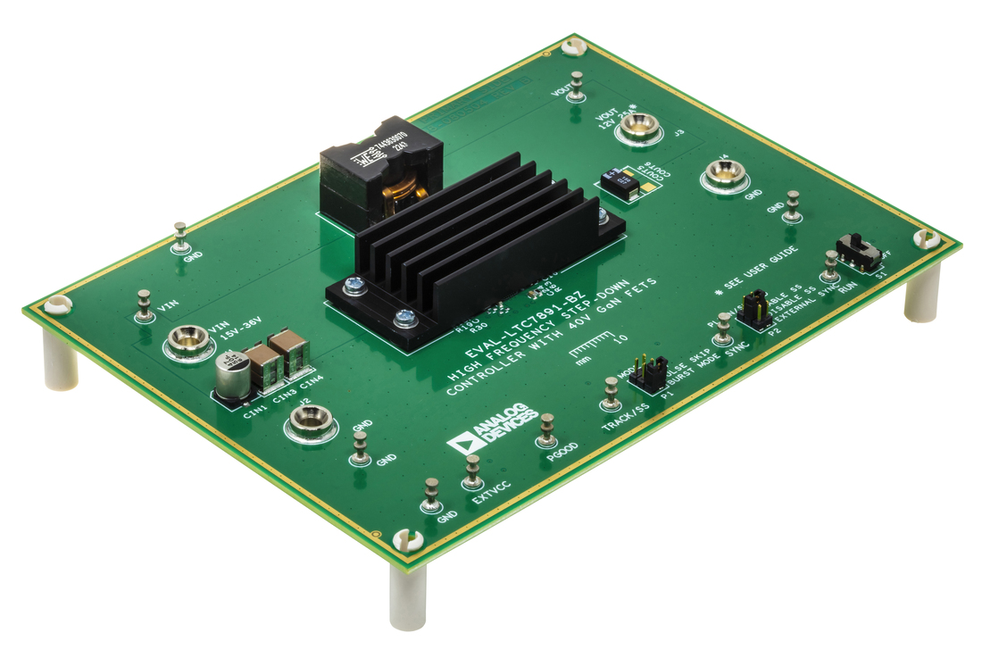
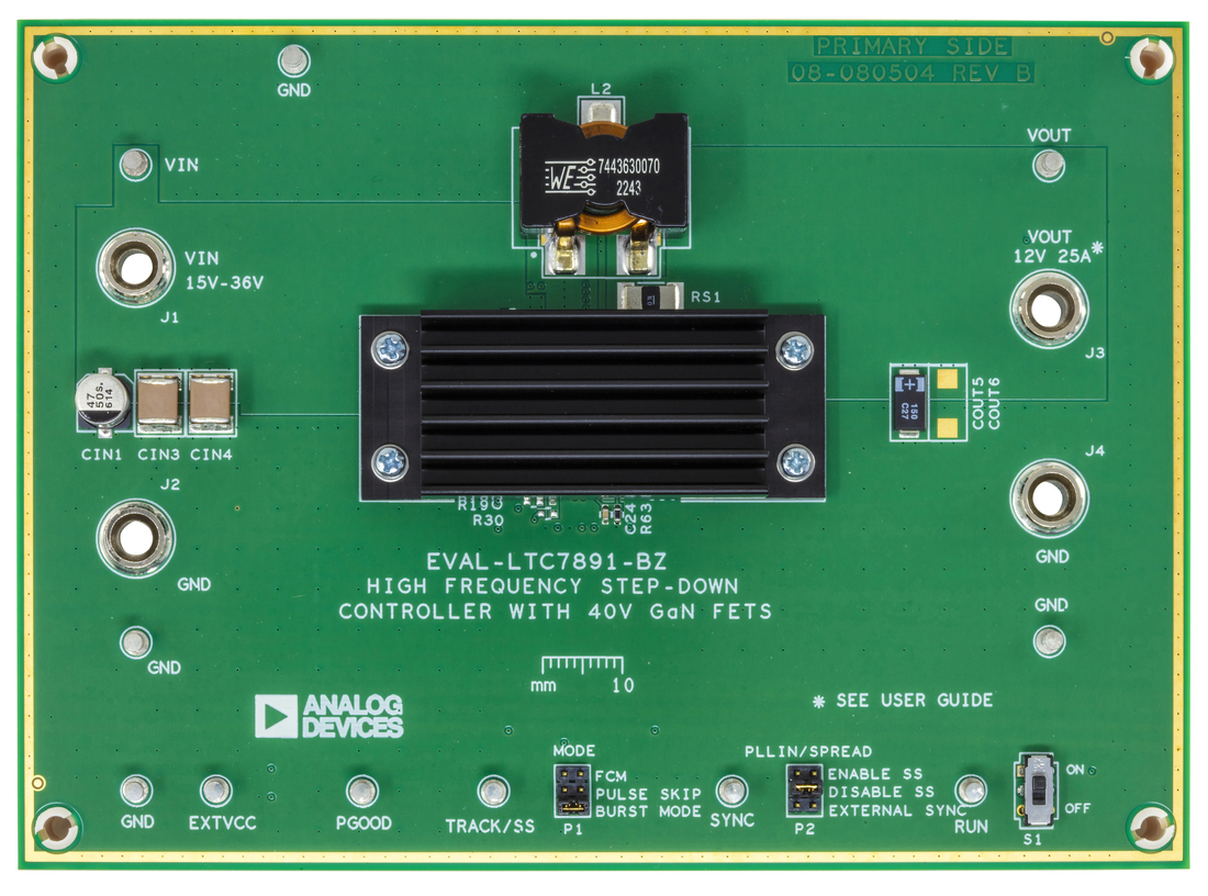
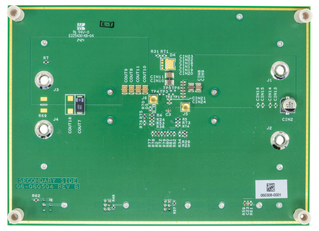
High Frequency Step-Down Controller with 40V GaN FETs
资料
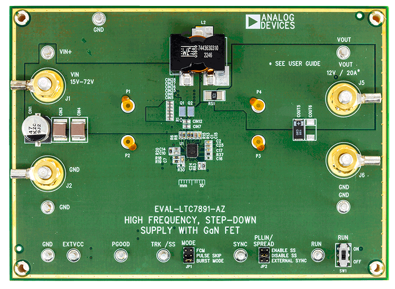
具有 EPC GaN FET 的高频降压型电源
资料
最新评论
需要发起讨论吗? 没有关于 LTC7891的相关讨论?是否需要发起讨论?
在EngineerZone®上发起讨论