LTC7149
推荐用于新设计用于提供负输出的 60V、4A、同步降压型稳压器
- 产品模型
- 8
产品详情
- 宽 VIN 范围:3.4V 至 60V
- 宽 VOUT 范围:0V 至 –28V
- 可采用单个电阻器设置 VOUT
- 集成型 110mΩ 上管 N 沟道 / 50mΩ 下管 N 沟道 MOSFET
- 稳定 IQ:440μA,停机 IQ:15μA
- 参考于电路板 GND 的 I/O 引脚 (RUN、PGOOD、MODE/SYNC)
- 准确的电阻器可编程频率 (300kHz 至 3MHz) 和 ±50% 的频率同步范围
- 12VIN 和 –5VOUT 时的效率达 92%
- ±0.8% 输出电压准确度
- 峰值电流模式操作
- 突发模式 (Burst Mode®) 操作,强制连续模式
- 可编程软起动
- 过热保护
- 采用 28 引脚 (4mm x 5mm) QFN 和 TSSOP 封装
LTC®7149 是一款面向负输出应用的高效率、60V、4A 同步单片式降压型稳压器。该稳压器具有可利用单个电阻器设置的输出电压,并可在宽 VOUT 范围内实现高效率。
这款负输出稳压器在 3.4V 至 60V 的输入电压范围内工作,并提供了一个从 –28V 至 0V 的可调输出范围,同时可输送高达 4A 的电感器电流。另外,开关频率还能利用一个外部电阻器进行调节。提供了一个用户可选的模式输入,以允许用户通过牺牲纹波噪声指标来换取轻负载时的效率提升;突发模式操作可在轻负载条件下提供最高的效率,而强制连续模式则可提供低输出纹波。MODE/SYNC 引脚还可用来使开关频率同步至一个外部时钟。内部电平移位电路允许使 I/O 引脚 (RUN、MODE/SYNC、PGOOD) 参考于电路板 GND。
LTC7149 的运作采用了一种峰值电流模式架构,其利用固有的逐周期电流限制保护特性实现了快速瞬态响应。
Applications
- 工业应用
- 电信电源
- 分布式电源系统
参考资料
数据手册 1
可靠性数据 1
用户手册 1
设计笔记 1
ADI 始终高度重视提供符合最高质量和可靠性水平的产品。我们通过将质量和可靠性检查纳入产品和工艺设计的各个范围以及制造过程来实现这一目标。出货产品的“零缺陷”始终是我们的目标。查看我们的质量和可靠性计划和认证以了解更多信息。
| 产品型号 | 引脚/封装图-中文版 | 文档 | CAD 符号,脚注和 3D模型 |
|---|---|---|---|
| LTC7149EFE#PBF | 28-Lead TSSOP w/ EP | ||
| LTC7149EFE#TRPBF | 28-Lead TSSOP w/ EP | ||
| LTC7149EUFD#PBF | 28-Lead QFN (4mm x 5mm x 0.75mm w/ EP) | ||
| LTC7149EUFD#TRPBF | 28-Lead QFN (4mm x 5mm x 0.75mm w/ EP) | ||
| LTC7149IFE#PBF | 28-Lead TSSOP w/ EP | ||
| LTC7149IFE#TRPBF | 28-Lead TSSOP w/ EP | ||
| LTC7149IUFD#PBF | 28-Lead QFN (4mm x 5mm x 0.75mm w/ EP) | ||
| LTC7149IUFD#TRPBF | 28-Lead QFN (4mm x 5mm x 0.75mm w/ EP) |
| 产品型号 | 产品生命周期 | PCN |
|---|---|---|
|
4月 6, 2022 - 22_0068 Laser Top Mark for ETSSOP and TSSOP Packages Assembled in ADPG [PNG] and UTL |
||
| LTC7149EFE#PBF | 量产 | |
| LTC7149EFE#TRPBF | 量产 | |
| LTC7149IFE#PBF | 量产 | |
| LTC7149IFE#TRPBF | 量产 | |
|
5月 17, 2019 - 19_0067 Notification of Wafer Fab Location Change for 0.35 BCD Process |
||
| LTC7149EFE#PBF | 量产 | |
| LTC7149EFE#TRPBF | 量产 | |
| LTC7149EUFD#PBF | 量产 | |
| LTC7149EUFD#TRPBF | 量产 | |
| LTC7149IFE#PBF | 量产 | |
| LTC7149IFE#TRPBF | 量产 | |
| LTC7149IUFD#PBF | 量产 | |
| LTC7149IUFD#TRPBF | 量产 | |
这是最新版本的数据手册
软件资源
找不到您所需的软件或驱动?
申请驱动/软件硬件生态系统
工具及仿真模型
LTspice 2
- LTC7149 Demo Circuit - Inverting Buck Regulator with Output Voltage Control (3.4-50Vin, 2.5 to -10Vout @ 2A)
- LTC7149 Demo Circuit - Inverting Buck Regulator (3.4-55V to -5V @ 2.5A)
LTspice中提供以下器件型号:
- LTC7149
LTpowerCAD 1
LTpowerCAD中提供以下器件的设计工具:
- LTC7149
LTspice®是一款强大高效的免费仿真软件、原理图采集和波形观测器,为改善模拟电路的仿真提供增强功能和模型。
LTpowerCAD®是一种电源设计程序,它选择功率级元件,提供详细效率信息,显示快速环路波特图稳定性和负载瞬态分析,并可导出至LTspice进行仿真。
评估套件
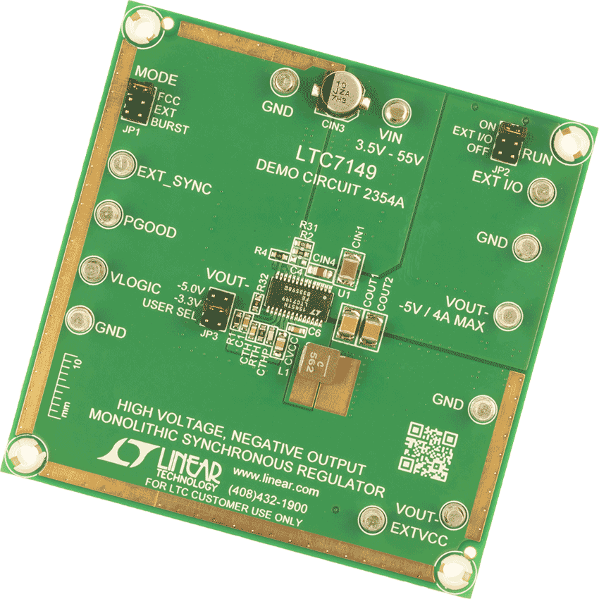
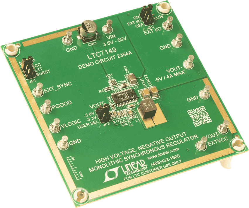
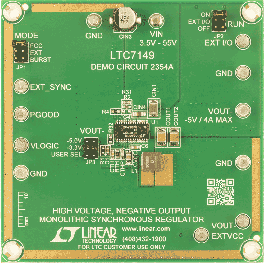
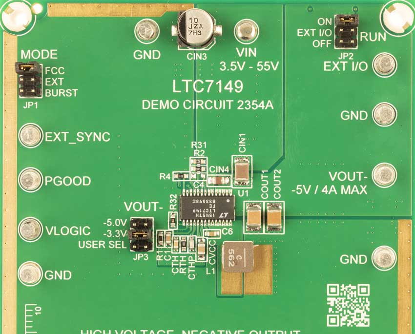
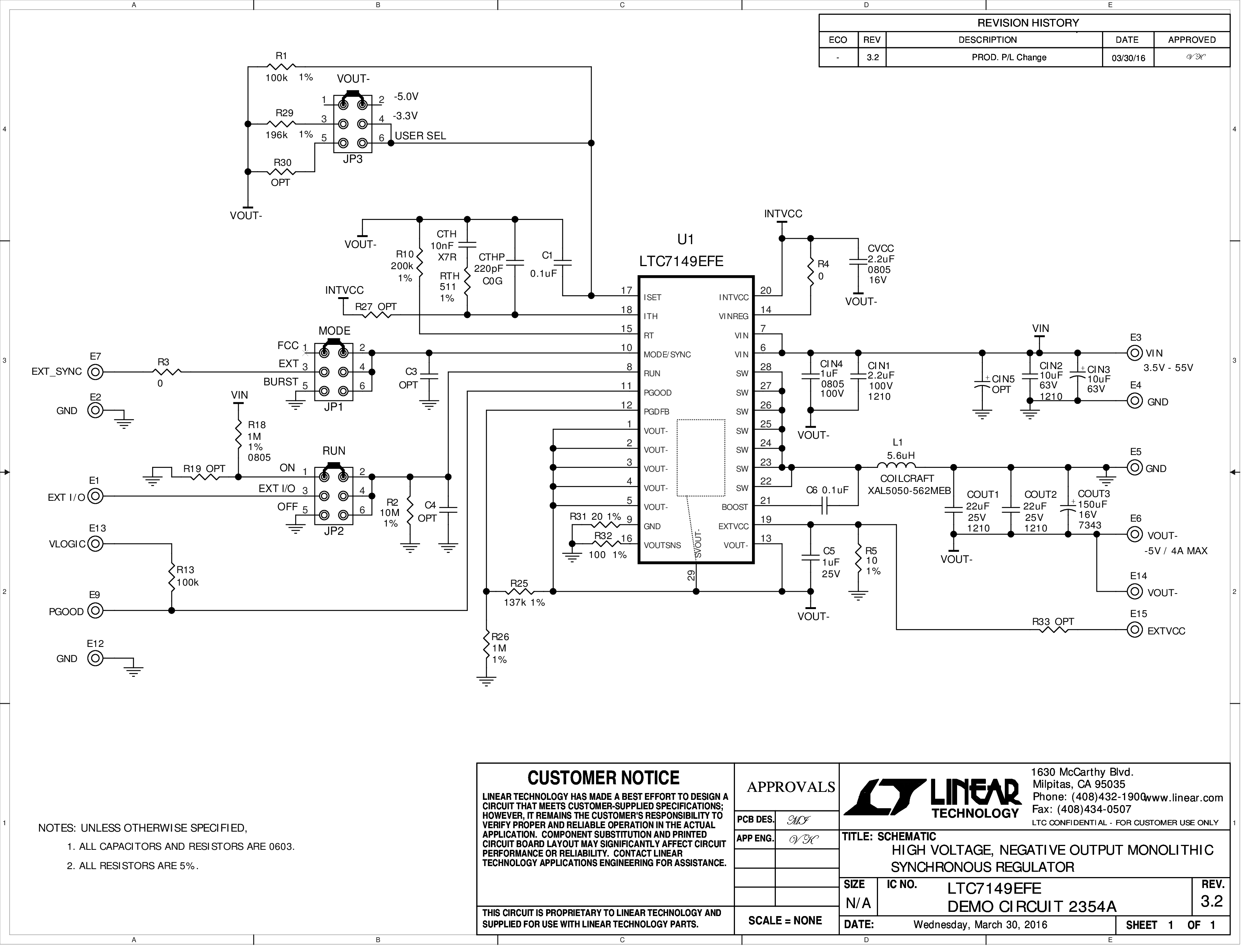
LTC7149 Demo Board | Buck Configured as Negative VOUT; 3.5V ≤ VIN ≤ 55V; VOUT = –3.3V/–5V/Adjustable to –56V @ up to 4A