LTC7000
LTC7000-1
推荐用于新设计
快速150V保护高端NMOS静态开关驱动器
- 产品模型
- 36
产品详情
- 宽工作VIN:3.5V至135V(绝对最大值为150V)
- 针对快速导通和关闭时间的1Ω下拉、2.2Ω上拉,具有35ns传播延迟
- 内部电荷泵,可实现100%占空比
- 短路保护
- 可调电流跳变阈值(LTC7000)
- 电流监控器输出(LTC7000)
- 自动重启定时器
- 开漏故障标志
- 可调导通压摆率
- 栅极驱动器电源电压为3.5V至15V
- 可调VIN欠压和过压闭锁(LTC7000)
- 可调驱动器电源VCC欠压闭锁
- 低关断电流:1µA
- CMOS兼容输入
- 散热增强型、支持高压的16引脚MSOP封装
- 通过AEC-Q100汽车应用认证
LTC7000/LTC7000-1是一款快速高端N通道MOSFET栅极驱动器,采用高达135V的输入电压工作。它包含一个内部电荷泵,可全面增强外部N通道MOSFET开关性能,使其无限保持导通状态。
其功能强大的驱动器可在极短的转换时间内轻松驱动大型栅极电容,因而非常适合需要快速导通和/或关断时间的高频开关应用或静态开关应用。
当内部比较器检测到开关电流超过预设电平时,故障标志置位,开关在外部定时电容设置的一段时间后关闭。冷却周期后,LTC7000/LTC7000-1自动重试。
LTC7000/LTC7000-1采用散热增强型16引脚MSOP封装。
| LTC7000 | LTC7000-1 | LTC7000A | LTC7000A-1 | |
| 封装 | 16引脚MSOP MSE16 | 16引脚MSOP MSE16(12) | 16引脚MSOP MSE16 | 16引脚MSOP MSE16(12) |
| 高压引脚间距 | 0.157mm | 0.657mm | 0.157mm | 0.657mm |
| RUN/OVLO/ISET/IMON引脚 | 是 | 否 | 是 | 否 |
| INP上升后IMON启用 | 150μsec | N/A | <1μsec | N/A |
应用
- 静态开关驱动器
- 负载和电源开关驱动器
- 电子阀驱动器
- 高频高端侧栅极驱动器
参考资料
数据手册 1
可靠性数据 1
用户手册 2
视频 2


产品选型卡 2
新闻 1
思想领导力 1
ADI 始终高度重视提供符合最高质量和可靠性水平的产品。我们通过将质量和可靠性检查纳入产品和工艺设计的各个范围以及制造过程来实现这一目标。出货产品的“零缺陷”始终是我们的目标。查看我们的质量和可靠性计划和认证以了解更多信息。
| 产品型号 | 引脚/封装图-中文版 | 文档 | CAD 符号,脚注和 3D模型 |
|---|---|---|---|
| LTC7000EMSE#PBF | 16-Lead MSOP w/ EP | ||
| LTC7000EMSE#TRPBF | 16-Lead MSOP w/ EP | ||
| LTC7000EMSE#WPBF | 16-Lead MSOP w/ EP | ||
| LTC7000EMSE#WTRPBF | 16-Lead MSOP w/ EP | ||
| LTC7000EMSE-1#PBF | 16(12)-Lead MSOP w/ EP | ||
| LTC7000EMSE-1#TRPBF | 16(12)-Lead MSOP w/ EP | ||
| LTC7000EMSE-1#WPBF | 16(12)-Lead MSOP w/ EP | ||
| LTC7000EMSE-1#WTRPBF | 16(12)-Lead MSOP w/ EP | ||
| LTC7000HMSE#PBF | 16-Lead MSOP w/ EP | ||
| LTC7000HMSE#TRPBF | 16-Lead MSOP w/ EP | ||
| LTC7000HMSE#WPBF | 16-Lead MSOP w/ EP | ||
| LTC7000HMSE#WTRPBF | 16-Lead MSOP w/ EP | ||
| LTC7000HMSE-1#PBF | 16(12)-Lead MSOP w/ EP | ||
| LTC7000HMSE-1#TRPBF | 16(12)-Lead MSOP w/ EP | ||
| LTC7000HMSE-1#WPBF | 16(12)-Lead MSOP w/ EP | ||
| LTC7000HMSE-1#WTRPBF | 16(12)-Lead MSOP w/ EP | ||
| LTC7000IMSE#PBF | 16-Lead MSOP w/ EP | ||
| LTC7000IMSE#TRPBF | 16-Lead MSOP w/ EP | ||
| LTC7000IMSE#WPBF | 16-Lead MSOP w/ EP | ||
| LTC7000IMSE#WTRPBF | 16-Lead MSOP w/ EP | ||
| LTC7000IMSE-1#PBF | 16(12)-Lead MSOP w/ EP | ||
| LTC7000IMSE-1#TRPBF | 16(12)-Lead MSOP w/ EP | ||
| LTC7000IMSE-1#WPBF | 16(12)-Lead MSOP w/ EP | ||
| LTC7000IMSE-1#WTRPBF | 16(12)-Lead MSOP w/ EP | ||
| LTC7000JMSE#PBF | 16-Lead MSOP w/ EP | ||
| LTC7000JMSE#TRPBF | 16-Lead MSOP w/ EP | ||
| LTC7000JMSE#WPBF | 16-Lead MSOP w/ EP | ||
| LTC7000JMSE#WTRPBF | 16-Lead MSOP w/ EP | ||
| LTC7000JMSE-1#PBF | 16(12)-Lead MSOP w/ EP | ||
| LTC7000JMSE-1#TRPBF | 16(12)-Lead MSOP w/ EP | ||
| LTC7000JMSE-1#WPBF | 16(12)-Lead MSOP w/ EP | ||
| LTC7000JMSE-1#WTRPBF | 16(12)-Lead MSOP w/ EP | ||
| LTC7000MPMSE#PBF | 16-Lead MSOP w/ EP | ||
| LTC7000MPMSE#TRPBF | 16-Lead MSOP w/ EP | ||
| LTC7000MPMSE-1#PBF | 16(12)-Lead MSOP w/ EP | ||
| LTC7000MPMSE-1#TRPBF | 16(12)-Lead MSOP w/ EP |
| 产品型号 | 产品生命周期 | PCN |
|---|---|---|
|
2月 4, 2020 - 20_0132 Laser Top Mark for 16-Lead MSOP Packages Assembled in ADPG and UTAC |
||
| LTC7000EMSE#PBF | 量产 | |
| LTC7000EMSE#TRPBF | 量产 | |
| LTC7000EMSE#WPBF | 量产 | |
| LTC7000EMSE#WTRPBF | 量产 | |
| LTC7000EMSE-1#WPBF | 量产 | |
| LTC7000EMSE-1#WTRPBF | 量产 | |
| LTC7000HMSE#PBF | 量产 | |
| LTC7000HMSE#TRPBF | 量产 | |
| LTC7000HMSE#WPBF | 量产 | |
| LTC7000HMSE#WTRPBF | 量产 | |
| LTC7000HMSE-1#WPBF | 量产 | |
| LTC7000HMSE-1#WTRPBF | 量产 | |
| LTC7000IMSE#PBF | 量产 | |
| LTC7000IMSE#TRPBF | 量产 | |
| LTC7000IMSE#WPBF | 量产 | |
| LTC7000IMSE#WTRPBF | 量产 | |
| LTC7000IMSE-1#WPBF | 量产 | |
| LTC7000IMSE-1#WTRPBF | 量产 | |
| LTC7000JMSE#PBF | 量产 | |
| LTC7000JMSE#TRPBF | 量产 | |
| LTC7000JMSE#WPBF | 量产 | |
| LTC7000JMSE#WTRPBF | 量产 | |
| LTC7000MPMSE#PBF | 量产 | |
| LTC7000MPMSE#TRPBF | 量产 | |
|
4月 17, 2025 - 25_0119 Bond Wire Change from Gold to Copper (Automotive) |
||
| LTC7000EMSE#WPBF | 量产 | |
| LTC7000EMSE#WTRPBF | 量产 | |
| LTC7000EMSE-1#PBF | 量产 | |
| LTC7000EMSE-1#TRPBF | 量产 | |
| LTC7000HMSE-1#PBF | 量产 | |
| LTC7000HMSE-1#TRPBF | 量产 | |
| LTC7000JMSE-1#PBF | 量产 | |
| LTC7000JMSE-1#TRPBF | 量产 | |
|
6月 5, 2024 - 24_0003 Epoxy Change from Henkel 8290 to 8290A for MSOP Package (2) |
||
| LTC7000EMSE-1#PBF | 量产 | |
| LTC7000EMSE-1#TRPBF | 量产 | |
| LTC7000HMSE-1#PBF | 量产 | |
| LTC7000HMSE-1#TRPBF | 量产 | |
| LTC7000IMSE-1#PBF | 量产 | |
| LTC7000IMSE-1#TRPBF | 量产 | |
| LTC7000JMSE-1#PBF | 量产 | |
| LTC7000JMSE-1#TRPBF | 量产 | |
| LTC7000MPMSE-1#PBF | 量产 | |
| LTC7000MPMSE-1#TRPBF | 量产 | |
|
2月 4, 2020 - 20_0129 Laser Mark Conversion for 12-Lead MSOP Packages Assembled in ADPG and UTAC |
||
| LTC7000EMSE-1#PBF | 量产 | |
| LTC7000EMSE-1#TRPBF | 量产 | |
| LTC7000EMSE-1#WPBF | 量产 | |
| LTC7000EMSE-1#WTRPBF | 量产 | |
| LTC7000HMSE-1#PBF | 量产 | |
| LTC7000HMSE-1#TRPBF | 量产 | |
| LTC7000HMSE-1#WPBF | 量产 | |
| LTC7000HMSE-1#WTRPBF | 量产 | |
| LTC7000IMSE-1#PBF | 量产 | |
| LTC7000IMSE-1#TRPBF | 量产 | |
| LTC7000IMSE-1#WPBF | 量产 | |
| LTC7000IMSE-1#WTRPBF | 量产 | |
| LTC7000JMSE-1#PBF | 量产 | |
| LTC7000JMSE-1#TRPBF | 量产 | |
| LTC7000JMSE-1#WPBF | 量产 | |
| LTC7000JMSE-1#WTRPBF | 量产 | |
| LTC7000MPMSE-1#PBF | 量产 | |
| LTC7000MPMSE-1#TRPBF | 量产 | |
|
10月 11, 2022 - 22_0244 Epoxy Change from Henkel 8290 to 8290A for MSOP Package |
||
| LTC7000EMSE-1#WPBF | 量产 | |
| LTC7000EMSE-1#WTRPBF | 量产 | |
| LTC7000HMSE-1#WPBF | 量产 | |
| LTC7000HMSE-1#WTRPBF | 量产 | |
| LTC7000IMSE-1#WPBF | 量产 | |
| LTC7000IMSE-1#WTRPBF | 量产 | |
| LTC7000JMSE-1#WPBF | 量产 | |
| LTC7000JMSE-1#WTRPBF | 量产 | |
|
10月 27, 2021 - 21_0154 Moisture Sensitivity Level Rating Change of LT8331, LTC3637, and LTC7000-1 with #W for MSOP Package |
||
| LTC7000EMSE-1#WPBF | 量产 | |
| LTC7000EMSE-1#WTRPBF | 量产 | |
| LTC7000HMSE-1#WPBF | 量产 | |
| LTC7000HMSE-1#WTRPBF | 量产 | |
| LTC7000IMSE-1#WPBF | 量产 | |
| LTC7000IMSE-1#WTRPBF | 量产 | |
| LTC7000JMSE-1#WPBF | 量产 | |
| LTC7000JMSE-1#WTRPBF | 量产 | |
|
6月 21, 2022 - 22_0050 UTAC Thai Limited (UTL) as Alternate Assembly Site for MSOP Packages / Devices |
||
| LTC7000HMSE-1#WPBF | 量产 | |
| LTC7000HMSE-1#WTRPBF | 量产 | |
这是最新版本的数据手册
软件资源
找不到您所需的软件或驱动?
申请驱动/软件硬件生态系统
工具及仿真模型
LTspice
LTspice中提供以下器件型号:
- LTC7000
- LTC7000-1
LTspice®是一款强大高效的免费仿真软件、原理图采集和波形观测器,为改善模拟电路的仿真提供增强功能和模型。
评估套件
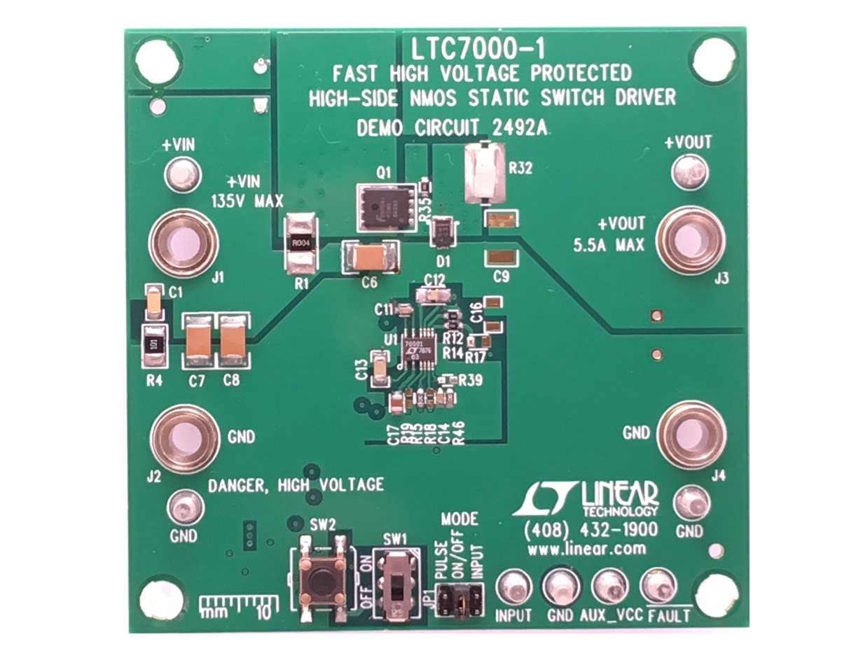
LTC7000-1 演示板高压侧保护的 NMOS 驱动器;8V ≤ VIN ≤ 135V,IOUT 高达 5.5A
资料
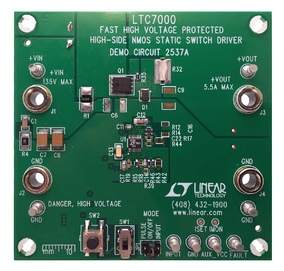
LTC7000 演示板高压侧受保护的 NMOS 驱动器;VIN 高达 135V,IOUT 高达 5.5A
资料


RF Front-end GaN Power Amplifier Biasing, Protection, and Control Reference Design
资料
软件
最新评论
需要发起讨论吗? 没有关于 LTC7000的相关讨论?是否需要发起讨论?
在EngineerZone®上发起讨论