ADPL54203
推荐新设计使用40VIN Micropower No-Opto Isolated Flyback Converter with 60V/3.4A Switch
- 产品模型
- 2
产品详情
- 3.4A, 60V Internal DMOS Power Switch
- 3.2V to 40V Input Voltage Range
- No Transformer Third Winding or Opto-Isolator Required for Output Voltage Regulation
- Quasi-Resonant Boundary Mode Operation at Heavy Load
- Low Ripple Burst Mode® Operation at Light Load
- Low Quiescent Current
- 115μA in Sleep Mode
- 390μA in Active Mode
- Minimum Load < 0.5% (Typ) of Full Output
- Temperature Compensation for Output Diode
- Internal Compensation and Soft-Start
- Output Short-Circuit Protection
- Accurate EN/UVLO Threshold and Hysteresis
- Thermally Enhanced 8-Lead SO Package
The ADPL54203 operates from an input voltage range of 3.2V to 40V and delivers up to 17W of isolated output power. It is a monolithic micropower isolated flyback converter. By sampling the isolated output voltage directly from the primary-side flyback waveform, the part requires no third winding or optoisolator for regulation. The output voltage is programmed with two external resistors and a third optional temperature compensation resistor. Boundary mode operation provides a small magnetic solution with excellent load regulation. Low ripple Burst Mode operation maintains high efficiency at light load while minimizing the output voltage ripple.
A 3.4A, 60V DMOS power switch is integrated along with all the high voltage circuitry and control logic into a thermally enhanced 8-lead SO package. The high level of integration and the use of boundary and low ripple burst modes result in a simple to use, low component count, and high efficiency application solution for isolated power delivery.
APPLICATIONS
- Isolated Auxiliary/Housekeeping Power Supplies
- Isolated Industrial, Medical Power Supplies
参考资料
数据手册 1
用户手册 1
视频 1

ADI 始终高度重视提供符合最高质量和可靠性水平的产品。我们通过将质量和可靠性检查纳入产品和工艺设计的各个范围以及制造过程来实现这一目标。出货产品的“零缺陷”始终是我们的目标。查看我们的质量和可靠性计划和认证以了解更多信息。
| 产品型号 | 引脚/封装图-中文版 | 文档 | CAD 符号,脚注和 3D模型 |
|---|---|---|---|
| ADPL54203ES8E#PBF | 8-Lead SOIC (Narrow 0.15 Inch w/ EP) | ||
| ADPL54203ES8E#TRPBF | 8-Lead SOIC (Narrow 0.15 Inch w/ EP) |
这是最新版本的数据手册
工具及仿真模型
LTspice 1
LTspice中提供以下器件型号:
- ADPL54203
LTspice®是一款强大高效的免费仿真软件、原理图采集和波形观测器,为改善模拟电路的仿真提供增强功能和模型。
评估套件
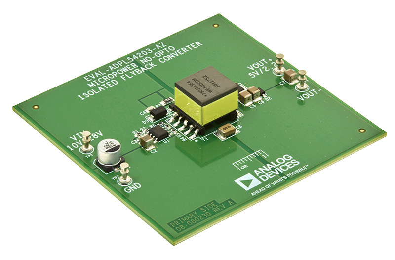
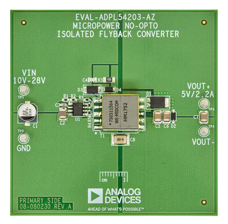
Micropower No-Opto Isolated Flyback Converter
资料
最新评论
需要发起讨论吗? 没有关于 adpl54203的相关讨论?是否需要发起讨论?
在EngineerZone®上发起讨论