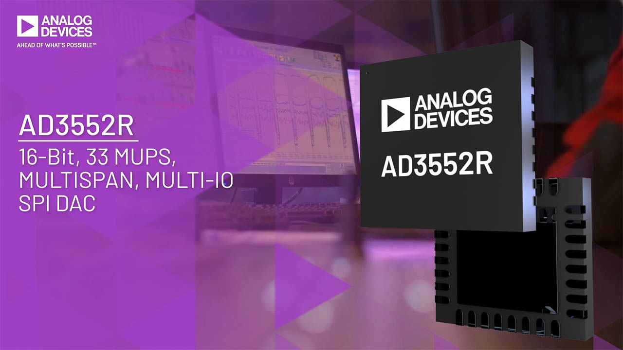
AD3552R
推荐新设计使用双路 16 位 33 MUPS 多跨度多 IO SPI DAC
- 产品模型
- 2
产品详情
- 16 位分辨率
- 快速模式下33 MUPS的单路速率
- 精确模式下 22 MUPS 的单路速率
- 小信号建立时间 65ns,精确度 0.1%
- 大信号建立时间 100ns,精确度 0.1%
- 超小毛刺:< 50 pV×s
- 超低时延:5 ns
- 总谐波失真:1 kHz 时为 −105 dB
- 配置度高的输出电压跨度和失调
- 1.2V 和 1.8V 逻辑电平兼容
- 单频段(经典)、双频段和四频段 SPI 模式
- 多个误差检测器,包括模拟和数字域
- 2.5 V 内部电压基准,10 ppm/°C 最大温度系数
- 5 mm × 5 mm LFCSP
AD3552R 是一款低漂移超快 16 位精确度的电流输出数模转换器 (DAC),可在多个电压跨度范围下配置。AD3552R 以 2.5 V 固定基准电压运行。
每个 DAC 包含 3 个漂移补偿反馈电阻器,用于所需的外部跨阻放大器 (TIA),对输出电压进行缩放。失调和增益缩放寄存器生成多个输出跨度范围,如 0V-2.5V、0V-5V、0V-10V、-5V - +5V、-10V - +10V,以及完整 16 位解析度的自定义中间范围。
DAC 可在快速模式下运行,从而实现最高速度;或者在精确模式下运行,从而实现最高精度。
串行外设接口 (SPI) 可配置为四 SPI 模式、双同步 SPI 模式、双 SPI 模式和单 SPI(经典 SPI)模式,支持单数据速率 (SDR) 或双数据速率 (DDR),逻辑电平为 1.2 V 至 1.8 V。
AD3552R 适应扩展的工业级温度范围(–40°C 至 +105°C)。
应用
- 仪器仪表
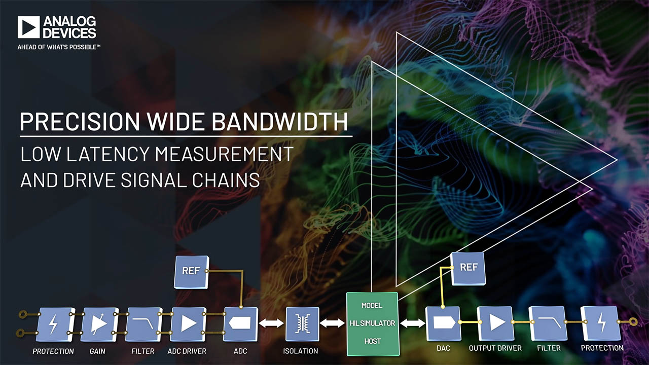
- 硬件在环
- 过程控制设备
- 医疗设备
- 自动测试设备
- 数据采集系统
- 可编程电压源
- 光通信
参考资料
数据手册 1
用户手册 1
视频 4


器件驱动器 6
ADI 始终高度重视提供符合最高质量和可靠性水平的产品。我们通过将质量和可靠性检查纳入产品和工艺设计的各个范围以及制造过程来实现这一目标。出货产品的“零缺陷”始终是我们的目标。查看我们的质量和可靠性计划和认证以了解更多信息。
| 产品型号 | 引脚/封装图-中文版 | 文档 | CAD 符号,脚注和 3D模型 |
|---|---|---|---|
| AD3552RBCPZ16 | 32-Lead LFCSP (5mm x 5mm x 0.95mm w/ EP) | ||
| AD3552RBCPZ16-RL7 | 32-Lead LFCSP (5mm x 5mm x 0.95mm w/ EP) |
这是最新版本的数据手册
软件资源
器件驱动器 6
Mbed支持 1
Evaluation Software 0
找不到您所需的软件或驱动?
硬件生态系统
工具及仿真模型
LTspice 1
LTspice中提供以下器件型号:
- AD3552R
IBIS 模型 1
LTspice®是一款强大高效的免费仿真软件、原理图采集和波形观测器,为改善模拟电路的仿真提供增强功能和模型。
评估套件


AD3552R-16的评估板是一款低漂移超快16位精确度的电流输出数模转换器(DAC)。
资料


RF Front-end GaN Power Amplifier Biasing, Protection, and Control Reference Design
资料
软件
参考电路


Quad Channel, Low Latency, Data Acquisition and Signal Generation Module
使用部分
资料
设计和集成工具
视频
-
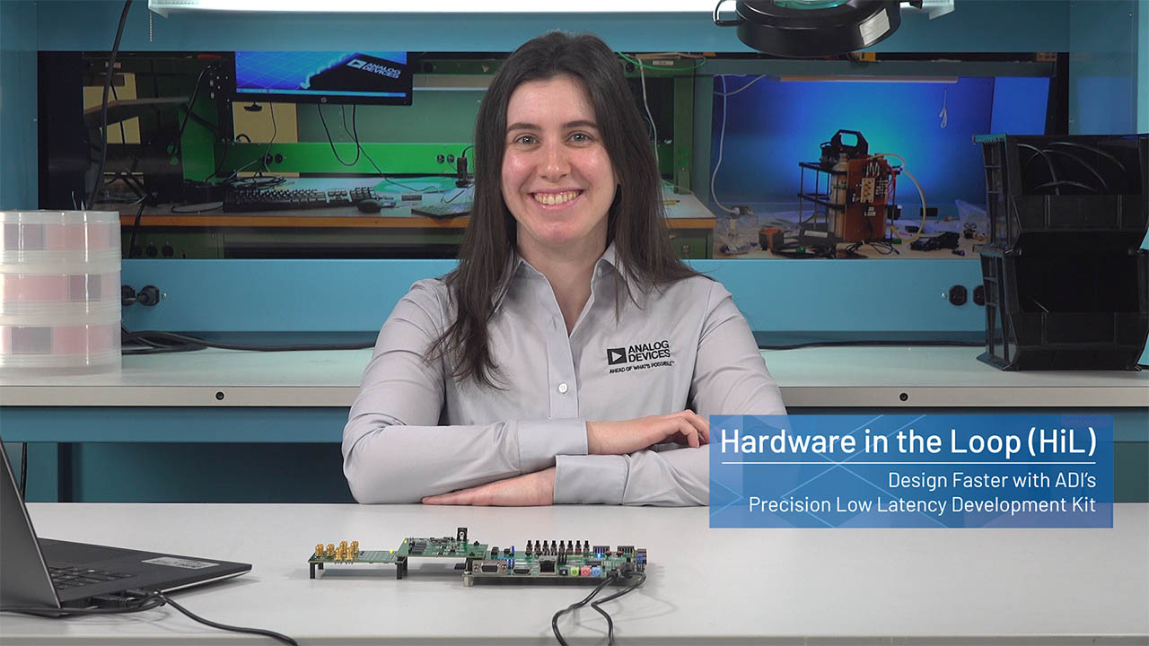 Low Latency Test and Measurement Kit – Hardware in the Loop
-
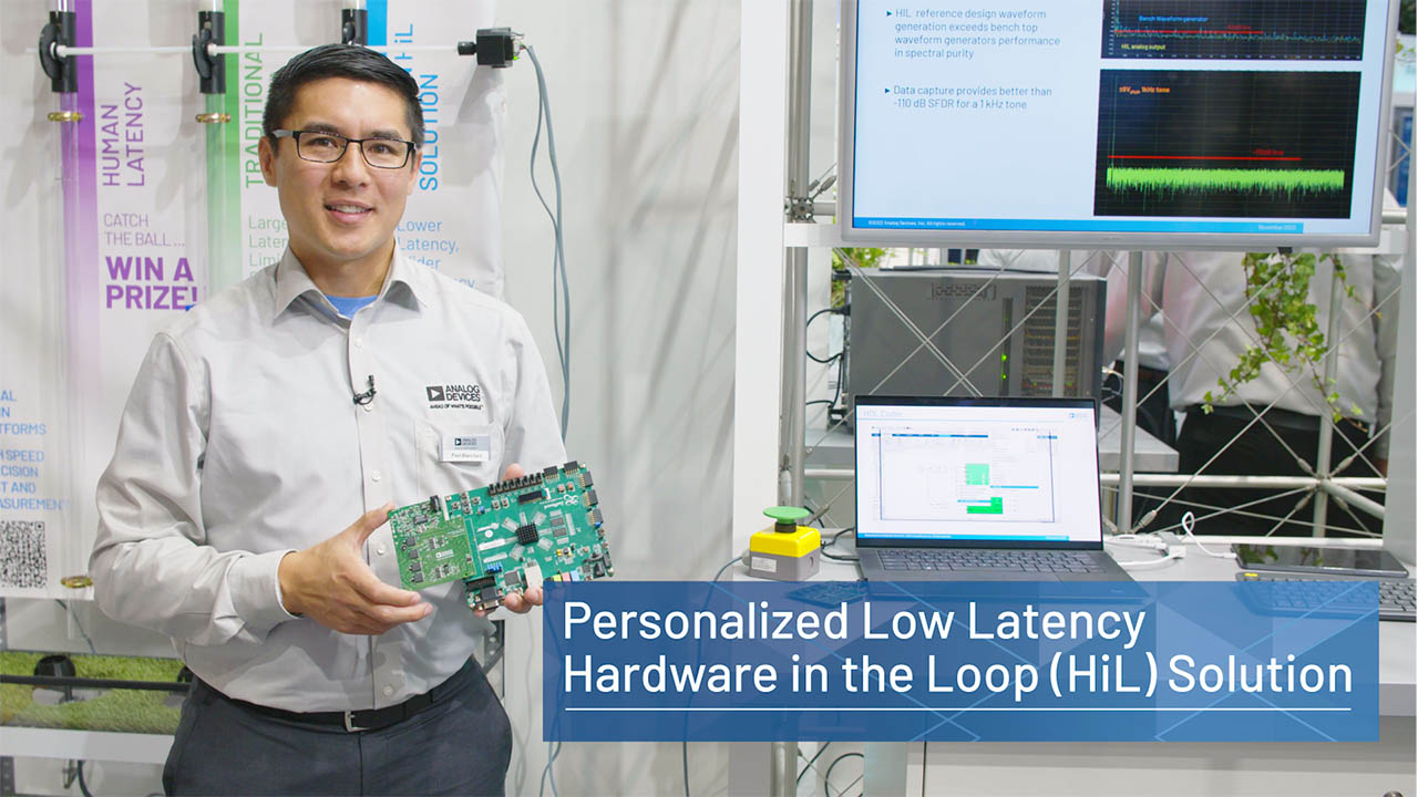 Personalized Low Latency Hardware in the Loop (HiL) Solution


Precision Low Latency Development Kit
使用部分
资料
设计和集成工具
视频
-
Low Latency Test and Measurement Kit – Hardware in the Loop
-
Personalized Low Latency Hardware in the Loop (HiL) Solution