
ADR4525
量产超低噪声、高精度2.5V基准电压源
- 产品模型
- 9
概述
- 最大温度系数(TCVOUT):
- 0.8 ppm/°C(D级,0°C至70°C)
- 1 ppm/°C(C级,0°C至70°C)
- 2 ppm/°C(B级,−40°C至+125°C)
- 4 ppm/°C(A级,−40°C至+125°C)
- 输出噪声(0.1 Hz至10 Hz):
- 1 μV p-p(VOUT为2.048 V(典型值)时)
- 初始输出电压误差:
- B、C、D级:±0.02%(最大值)
- 输入电压范围:3 V至15 V
- 工作温度范围:
- A级和B级:−40°C至+125°C
- C 级和 D 级:0°C 至 +70°C
- 输出电流:+10 mA拉电流/-10 mA灌电流
- 低静态电流:950 µA(最大值)
- 低压差:300 mV(2 mA,VOUT ≥ 3 V)
- 8引脚SOIC封装和LCC封装
- 通过AEC-Q100汽车应用认证
- 长期漂移:8 ppm(典型值)/4500小时
ADR4520/ADR4525/ADR4530/ADR4533/ADR4540/ADR4550器件均为高精度、低功耗、低噪声基准电压源,B、C和D级的最大初始误差为±0.02%,并具有出色的温度稳定性和低输出噪声。
该系列基准电压源使用创新的内核拓扑结构来实现高精度,同时提供出色的温度稳定性和噪声性能。这些器件具有较低的热感应输出电压滞回,并且长期输出电压漂移低,从而提高了时间和温度变化下的系统精度。
最大工作电流为950μA,最大压差低至300 mV,因此非常适合便携式设备应用。
ADR4520/ADR4525/ADR4530/ADR4533/ADR4540/ADR4550系列基准电压源采用8引脚SOIC封装,可提供较宽的输出电压范围,所有器件的额定温度范围均为−40°C至+125°C扩展工业温度范围。
ADR4525、ADR4540和ADR4550也提供D级(采用8引脚LCC封装)和C级,温度范围为0°C至70°C。ADR4525W采用8引脚SOIC封装,适合汽车应用。
应用
- 精密数据采集系统
- 高分辨率数据转换器
- 高精度测量器件
- 工业仪器仪表
- 医疗设备
- 汽车电池监控
参考资料
数据手册 2
应用笔记 3
技术文章 1
视频 7


参考电路 4
3rd Party Solutions 1
模拟对话 1
ADI 始终高度重视提供符合最高质量和可靠性水平的产品。我们通过将质量和可靠性检查纳入产品和工艺设计的各个范围以及制造过程来实现这一目标。出货产品的“零缺陷”始终是我们的目标。查看我们的质量和可靠性计划和认证以了解更多信息。
| 产品型号 | 引脚/封装图-中文版 | 文档 | CAD 符号,脚注和 3D模型 |
|---|---|---|---|
| ADR4525ARZ | 8-Lead SOIC | ||
| ADR4525ARZ-R7 | 8-Lead SOIC | ||
| ADR4525BRZ | 8-Lead SOIC | ||
| ADR4525BRZ-R7 | 8-Lead SOIC | ||
| ADR4525CRZ | 8-Lead SOIC | ||
| ADR4525CRZ-R7 | 8-Lead SOIC | ||
| ADR4525DEZ | LCC | ||
| ADR4525DEZ-R7 | LCC | ||
| ADR4525WBRZ-R7 | 8-Lead SOIC |
这是最新版本的数据手册
硬件生态系统
| 部分模型 | 产品周期 | 描述 |
|---|---|---|
| 线性稳压器 1 | ||
| LT3040 | 推荐用于新设计 | 20V、200mA、超低噪声、超高 PSRR 精准 DAC/基准缓冲器 |
工具及仿真模型
LTspice
LTspice中提供以下器件型号:
- ADR4525
Signal Chain Designer
Signal Chain Designer is a web-based tool designed to create and simulate complex precision signal chains. See your circuit’s performance before you commit to your PCB: transfer function, noise, power consumption, input range, and DC error. Quickly experiment with different parts and architectures. Signal chains can be exported to LTspice for further analysis.
打开工具
LTspice®是一款强大高效的免费仿真软件、原理图采集和波形观测器,为改善模拟电路的仿真提供增强功能和模型。
评估套件

Evaluation Board for the AD5676R WLCSP
资料


RF Front-end GaN Power Amplifier Biasing, Protection, and Control Reference Design
资料
软件
参考电路


16 位、100 kSPS 单电源低功耗数据采集系统
使用部分
设计和集成工具


16位单电源LED电流驱动器,积分和差分非线性误差小于±1 LSB
使用部分
设计和集成工具


带可编程增益跨阻放大器和同步检波器的双通道色度计
使用部分
资料
设计和集成工具


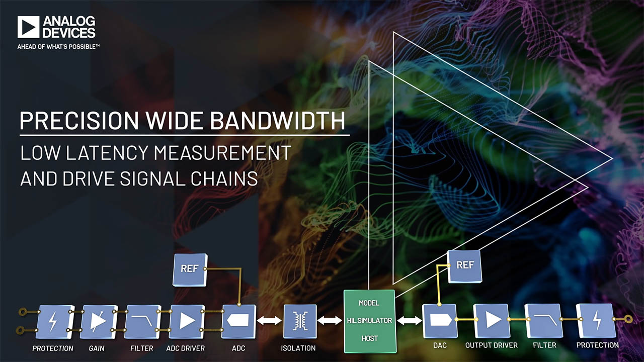
Quad Channel, Low Latency, Data Acquisition and Signal Generation Module
使用部分
资料
设计和集成工具
视频
-
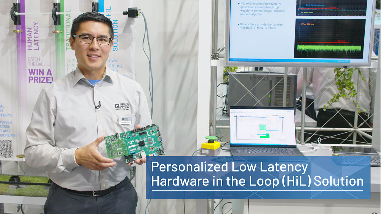 Personalized Low Latency Hardware in the Loop (HiL) Solution
-
 低延迟测试和测量套件 – HiL
-
 Low Latency Test and Measurement Kit – Hardware in the Loop


±10 V 模拟输入和±15 V 模拟输出,适用于树莓派平台
使用部分
资料
设计和集成工具
视频
-
 CN0554: 10V Analog Input and 15V Analog Output for Raspberry Pi


超高灵敏度飞安测量平台
使用部分
设计和集成工具
视频
-
sample_iTunes
-
Valeria
-
AnalogDevices-F04