CN0194


Overview
Design Resources
Design & Integration File
- Schematic
- Bill of Materials
- Gerber Files
- PADS Files
- Assembly Drawing
Evaluation Hardware
Part Numbers with "Z" indicate RoHS Compliance. Boards checked are needed to evaluate this circuit.
- EVAL-CFTL-6V-PWRZ ($20.01) Wall Power Supply for Eval Board
- EVAL-CN0194-SDPZ ($74.90) Galvanically Isolated, 2-Channel, 16-Bit, Simultaneous Sampling, Daisy-Chained Data Acquisition System
- EVAL-SDP-CB1Z ($116.52) Eval Control Board SDP
Device Drivers
Software such as C code and/or FPGA code, used to communicate with component's digital interface.
Features & Benefits
- Simultaneous sampling
- Isolated high speed analog to digital conversion
- Level shift and attenuates +/- 10 V industrial signal
Product Categories
Markets and Technologies
Parts Used
Documentation & Resources
-
CN0194 Software User Guide10/18/2018WIKI
-
MT-101: Decoupling Techniques2/14/2015PDF954 kB
-
MT-073: High Speed Variable Gain Amplifiers2/14/2015PDF177 kB
-
MT-031: Grounding Data Converters and Solving the Mystery of "AGND" and "DGND"3/20/2009PDF144 kB
Circuit Function & Benefits
This circuit, shown in Figure 1, provides galvanic isolation for
high speed, high accuracy, simultaneous sampling analog-todigital
conversion applications. The 16-bit AD7685 PulSAR ADC is versatile and allows monitoring of multiple channels through daisy chaining. An input circuit based on the AD8615 op amp level shifts, attenuates, and buffers a ±10 V industrial signal to match the input requirements of the ADC. The flexible circuit includes a precision ADR391 reference and two quadchannel ADuM1402 digital isolators to provide a compact and cost effective solution to a popular industrial data acquisition
application.


Circuit Description
The AD7685 is a 16-bit, charge redistribution successive approximation (SAR) analog-to-digital converter (ADC) that operates from a single VDD power supply from 2.3 V to 5.5 V. It contains a low power, high speed, 16-bit sampling ADC with no missing codes, no pipeline delay, an internal conversion clock, and a versatile serial interface port. The ADC also contains a low noise, wide bandwidth, short aperture delay, track-and-hold circuit. On the CNV rising edge, it samples an analog input (IN+) between 0 V to VREF with respect to the ground sense (IN−). The reference voltage, VREF, is applied externally and is set from 0.5 V to VDD. The circuit of Figure 1 uses a 4.5 V reference voltage.
Power dissipation of the AD7685 scales linearly with sampling rate. Power dissipation is 15 mW maximum for VDD = 5 V and a sampling rate of 250 kSPS. The AD7685 is housed in a 10-lead MSOP or a 10-lead QFN (LFCSP) with operation specified from −40°C to +85°C. The SPI-compatible serial interface also features the ability, using the SDI input, to either daisy chain several ADCs on a single 3-wire bus or provide an optional BUSY indicator. It is compatible with 1.8 V, 2.5 V, 3 V, or 5 V logic using the separate VIO supply pin.
The complete analog signal chain runs on a single 5 V supply. The ADR391 low dropout 2.5 V reference and the U13 rail-torail CMOS AD8615 op amp develop the 4.5 V reference voltage for the ADCs. A 4.5 V reference gives 0.5 V headroom at the output of U13 so that the op amp remains in the linear region for nominal variations in the 5 V supply. The ADR391 2.5 V output is amplified by the noise gain of U13, which is 1 + R4/R5. For the R4 and R5 values chosen, the noise gain is 1.8, and the reference voltage is 1.8 × 2.5 V = 4.5 V.
The U4 and U14 AD8615 op amps provide a signal gain of 0.225 (set by the ratio of R1 to R2 and R19 to R20), which reduces the amplitude of the 20 V p-p input signals to 4.5 V p-p at the inputs of the ADCs. A 2.25 V offset is required at the outputs of U4 and U14 for a 0 V input. This requires a commonmode voltage of 1.84 V at the noninverting input of U4 and U14. This voltage is developed by the resistor divider R3-R6.
The R-C network on the output of U4 and U14 (33 Ω, 2.7 nF) forms a single-pole noise filter with a bandwidth of 1.8 MHz.
The AD8615 is a CMOS rail-to-rail input and output, singlesupply amplifier featuring very low offset voltage, wide signal bandwidth, and low input voltage and current noise. The part uses a patented DigiTrim® trimming technique that achieves superior precision without laser trimming. The AD8615 is fully specified to operate from 2.7 V to 5 V single supplies.
The combination of greater than 20 MHz bandwidth, low offset, low noise, and low input bias current makes this amplifier useful in a wide variety of applications. Filters, integrators, photodiode amplifiers, and high impedance sensors all benefit from the combination of performance features. AC applications benefit from the wide bandwidth and low distortion. The AD8615 offers the highest output drive capability of the DigiTrim family, which is excellent for audio line drivers and other low impedance applications.
Applications for the parts include portable and low powered instrumentation, audio amplification for portable devices, portable phone headsets, barcode scanners, and multipole filters. The ability to swing rail-to-rail at both the input and output enables designers to buffer CMOS ADCs, DACs, ASICs, and other wide output swing devices in single-supply systems.
The ADR391 micropower, low dropout voltage reference provides a stable output voltage from a minimum supply of 300 mV above the output. Its advanced design eliminates the need for external capacitors, which further reduces board space and system cost. The combination of low power operation, small size, and ease of use makes the ADR391 precision voltage reference ideally suited for battery-operated applications. Using patented temperature drift curvature correction techniques from Analog Devices, the ADR391 reference achieves a low 9 ppm/°C of temperature drift in a TSOT package.
The ADuM1402 is a quad-channel digital isolator based on Analog Devices’ iCoupler® technology. Combining high speed CMOS and monolithic air core transformer technology, this isolation component provides outstanding performance characteristics superior to alternatives such as optocoupler devices.
By avoiding the use of LEDs and photodiodes, iCoupler devices remove the design difficulties commonly associated with optocouplers. The typical optocoupler concerns regarding uncertain current transfer ratios, nonlinear transfer functions, and temperature and lifetime effects are eliminated with the simple iCoupler digital interfaces and stable performance characteristics.
The need for external drivers and other discrete components is eliminated with these iCoupler products. Furthermore, iCoupler devices consume one-tenth to one-sixth of the power of optocouplers at comparable signal data rates.
The ADuM1402 isolators provides four independent isolation channels with 2/2 directionality and multiple data rates up to 90 Mbps for the C grade (see the data sheet Ordering Guide). All models operate with the supply voltage on either side ranging from 2.7 V to 5.5 V, providing compatibility with lower voltage systems, as well as enabling a voltage translation functionality across the isolation barrier. In addition, the ADuM1402 provides low pulse width distortion (<2 ns) and tight channel-to-channel matching (<2 ns). Unlike other optocoupler alternatives, the ADuM1402 isolators have a patented refresh feature that ensures dc correctness in the absence of input logic transitions and when power is not applied to one of the supplies.
Figure 1 shows how the AD7685’s are daisy-chained to reduce the number of signals requiring isolation. Note that the RSCLK and RFS are readbacks of the AD7685’s serial clock (SCK) and serial frame sync (CNV), respectively. These readback signals need to have a very short skew with respect to the DATA signal. This skew is the channel-to-channel matching propagation delay of the digital isolator (tPSKCD), which is less than 2 ns for the ADuM1402C. This allows running the serial interface at the maximum speed of the digital isolator (90 Mbps for the ADuM1402C), which corresponds to a maximum serial clock frequency of 90 MHz. This might have been otherwise limited by the cascade of the propagation delays of the digital isolators if the delays were too long. In the circuit, the TSCLK frequency is 30 MHz for a sampling frequency of 250 kSPS.
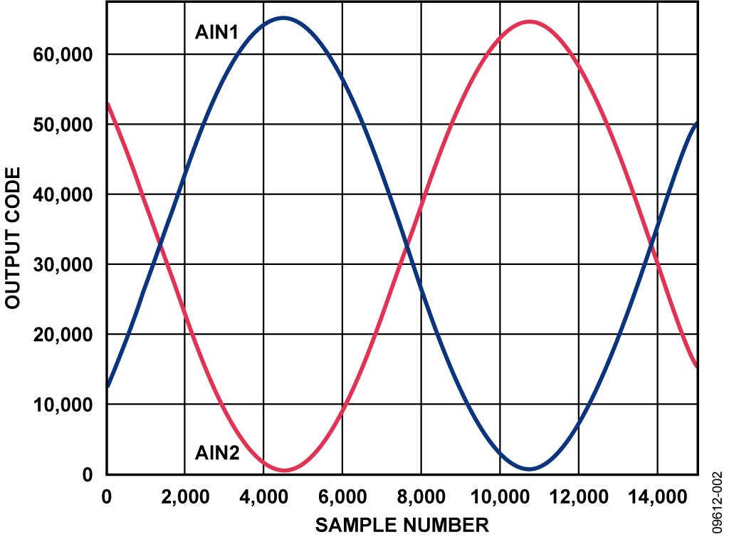
Two ±10 V signals 90° out of phase were applied to the two channels (AIN1 and AIN2) of the EVAL-CN0194-SDPZ board. The results of their conversion are seen in Figure 2, which was obtained using the supplied evaluation software. The supplied evaluation software can also be used to view FFT data (Figure 3) as well as a histogram for codes at a fixed dc level (Figure 4).
The performance of this or any high speed circuit is highly dependent on proper PCB layout. This includes, but is not limited to, power supply bypassing, controlled impedance lines (where required), component placement, signal routing, and power and ground planes. (See MT-031 Tutorial, MT-101 Tutorial, and the article, A Practical Guide to High-Speed Printed-Circuit-Board Layout, for more detailed information regarding PCB layout.)
A complete design support package for this circuit note can be found at www.analog.com/CN0194-DesignSupport.


Common Variations
Other pin-compatible 16-bit ADCs in the PulSAR family are available at higher sampling rates: AD7686 (500 kSPS), AD7980 (1 MSPS), and AD7983 (1.33 MSPS). If 18-bit resolution is needed, the following are also pin-compatible members of the PulSAR family: AD7691 (250 kSPS), AD7690 (500 kSPS), AD7982 (1 MSPS), and AD7984 (1.33 MSPS). The AD8615 op amp is also available in dual (AD8616) and quad (AD8618) package versions. Other possible driver op amps are the ADA4841-1 (single), ADA4841-2 (dual), and ADA4941-1 (dual differential).
Circuit Evaluation & Test
This circuit uses the EVAL-CN0194-SDPZ circuit board and the EVAL-SDP-CB1Z System Demonstration Platform (SDP) evaluation board. The two boards have 120-pin mating connectors, allowing for the quick setup and evaluation of the circuit’s performance. The EVAL-CN0194-SDPZ board contains the circuit to be evaluated, as described in this note, and the SDP evaluation board is used with the CN0194 evaluation software to capture the data from the EVAL-CN0194-SDPZ circuit board.
Equipment Needed
- PC with a USB port and Windows® XP, Windows Vista (32-bit), or Windows 7 (32-bit)
- EVAL-CN0194-SDPZ circuit evaluation board
- EVAL-SDP-CB1Z SDP evaluation board
- Power supply: +6 V, or +6 V “wall wart”
- Low distortion signal source, such as Audio Precision System Two 2322
Getting Started
Load the evaluation software by placing the CN0194 Evaluation Software disc in the CD drive of the PC. Using "My Computer," locate the drive that contains the evaluation software disc and open the Readme file. Follow the instructions contained in the Readme file for installing and using the evaluation software.
Functional Block Diagram
See Figure 1 of this circuit note for the circuit block diagram, and the PDF file “EVAL-CN0194-SDPZ-SCH" for the circuit schematics. This file is contained in the CN0194 DesignSupport Package.
Setup
Connect the 120-pin connector on the EVAL-CN0194-SDPZ circuit board to the connector marked “CON A” on the EVAL-SDP-CB1Z evaluation (SDP) board. Nylon hardware should be used to firmly secure the two boards, using the holes provided at the ends of the 120-pin connectors. With power to the supply off, connect a +6 V power supply to the pins marked “+6V CFTL” and “+6 V SDP” on the board. If available, a +6 V "wall wart" can be connected to the barrel jack connector on the board and used in place of the +6 V power supply. Connect the USB cable supplied with the SDP board to the USB port on the PC. Note: Do not connect the USB cable to the mini USB connector on the SDP board at this time.
Test
Apply power to the +6 V supply (or “wall wart”) connected to the EVAL-CN0194-SDPZ circuit board. Launch the evaluation software, and connect the USB cable from the PC to the USB mini connector on the SDP board. The software will be able to communicate to the SDP board if the Analog Devices System Development Platform driver is listed in the Device Manager.
Once USB communications are established, the SDP board can be used to send, receive, and capture serial data from the EVAL-CN0194-SDPZ board.
The data in this circuit note were generated using an Audio Precision System Two 2322 signal source and a GlobTek power supply. The signal source was set to the frequencies indicated in the graphs.
Information regarding the SDP board can be found at www.analog.com/SDP.