AD4632-16
新規設計に推奨16-Bit, 500 kSPS, Dual Channel SAR ADC
- 製品モデル
- 2
- 1Ku当たりの価格
- 最低価格:$13.86
製品の詳細
- High performance
- Throughput: 500 kSPS per channel maximum
- INL: ±3 ppm maximum from −40°C to +125°C
- SNR: 97.4 dB typical
- THD: −127 dB typical
- NSD: −157.4 dBFS/Hz typical
- Low power
- 15 mW per channel at 2 MSPS
- 5 mW per channel at 500 kSPS
- 1.5 mW per channel at 10 kSPS
- Easy Drive features reduce system complexity
- Low 0.6 μA input current for dc inputs
- Wide common-mode input range: −(1/128) × VREF to +(129/128) × VREF
- Flexible external reference voltage range: 4.096 V to 5 V
- Accurate integrated reference buffer with 2 μF bypass capacitor
- Programmable block averaging filter with up to 216 decimation
- Extended sample resolution to 30 bits
- Over range and synchronization bits
- Flexi-SPI digital interface
- 1, 2, or 4 SDO lanes per channel allows slower SCK
- Echo clock mode simplifies use of digital isolator
- Compatible with 1.2 V to 1.8 V logic
- 7 mm × 7 mm 64-Ball CSP_BGA package with internal supply and reference capacitors to help reduce system footprint
The AD4630-16/AD4632-16 are 2-channel, simultaneous sampling, Easy Drive™, 2 MSPS or 500 kSPS successive approximation register (SAR), analog-to-digital converters (ADCs). With a guaranteed maximum ±3 ppm integral nonlinearity (INL) and no missing codes at 16-bits, the AD4630-16/AD4632-16 achieve excellent precision from −40°C to +125°C. Figure 1 in the data sheet shows the functional architecture of the AD4630-16/AD4632-16.
A low-drift, internal precision-reference buffer eases voltage-reference sharing with other system circuitry. The AD4630-16/AD4632-16 offer a typical dynamic range of 97.4 dB when using a 5 V reference. The low noise floor enables signal chains utilizing less gain and lower power. A block averaging filter with programmable decimation ratio is available and can reduce noise for low-bandwidth signals, improving accuracy. The wide differential input and common-mode ranges allow inputs to use the full voltage reference (±VREF) range without saturating, simplifying signal-conditioning requirements and system calibration. The improved settling of the Easy Drive analog inputs broadens the selection of analog front end (AFE) components compatible with the AD4630-16/AD4632-16. Both single-ended and differential signals are supported.
The versatile Flexi-SPI serial-peripheral interface (SPI) eases host processor and ADC integration. A wide data-clocking window, multiple serial-data output (SDO) lanes, and optional dual data rate (DDR) data clocking can reduce the serial clock to 10 MHz while operating at a sample rate of 2 MSPS. Echo clock mode can relax the timing requirements and simplify the use of digital isolators.
The ball grid array (BGA) package of the AD4630-16/AD4632-16 integrates all critical power supply and reference bypass capacitors, reducing the footprint and system-component count, and lessening sensitivity to board layout.
APPLICATIONS
- Automatic test equipment
- Digital control loops
- Medical instrumentation
- Seismology
- Semiconductor manufacturing
- Scientific instrumentation
ドキュメント
データシート 1
ユーザ・ガイド 2
ビデオ 2
デバイス・ドライバ 1
| 製品モデル | ピン/パッケージ図 | 資料 | CADシンボル、フットプリント、および3Dモデル |
|---|---|---|---|
| AD4632-16BBCZ | 64-Lead BGA (7 mm x 7 mm x 1.72 mm) | ||
| AD4632-16BBCZ-RL | 64-Lead BGA (7 mm x 7 mm x 1.72 mm) |
これは最新改訂バージョンのデータシートです。
ソフトウェア・リソース
FPGA/HDL 1
デバイス・ドライバ 1
評価用ソフトウェア 0
必要なソフトウェア/ドライバが見つかりませんか?
ツールおよびシミュレーション
LTspice 1
高精度ADC ドライバ・ツール
高精度ADCドライバ・ツールは、高精度ADCとドライバを組み合わせたときの性能をシミュレートするWebアプリケーションです。ドライバの選択、キックバックのセトリング、歪みの潜在的な問題を明らかにし、設計のトレードオフを短時間で評価できます。システム・ノイズ、歪み、ADC入力のセトリングについてシミュレーションと計算ができます。
ツールを開くIBISモデル 1
Signal Chain Designer – BETA版
Signal Chain Designerは、複雑な高精度シグナル・チェーンの構築、シミュレーションを行うために設計されたウェブベースのツールです。PCBを作成する前に、伝達関数、ノイズ、消費電力、入力範囲、DCエラーなど、回路の性能を確認できます。さまざまな部品やアーキテクチャを素早く試すことができます。シグナル・チェーンはLTspiceにエクスポートして更に解析を行うことができます。
ツールを開く
LTspice®は、無料で提供される強力で高速な回路シミュレータと回路図入力、波形ビューワに改善を加え、アナログ回路のシミュレーションを容易にするためのモデルを搭載しています。
評価用キット
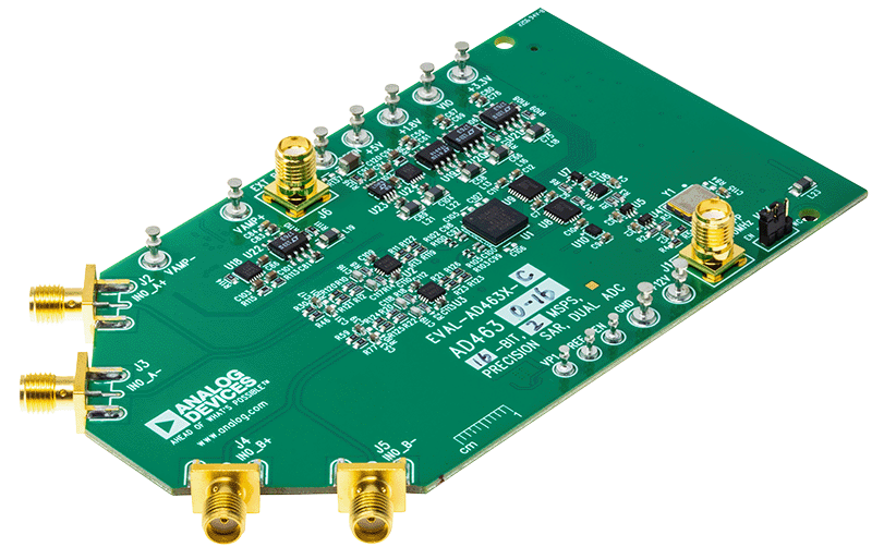
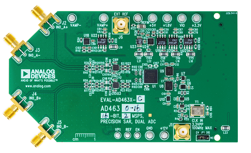
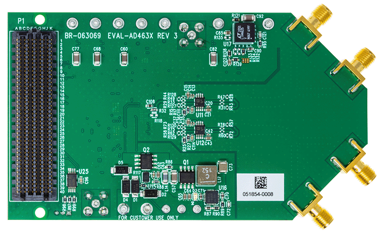
AD4630-16 SAR ADC Evaluation Board
資料
ソフトウェア
最新のディスカッション
AD4632-16に関するディスカッションはまだありません。意見を投稿しますか?
EngineerZone®でディスカッションを始める