CN0360


Overview
Design Resources
Design & Integration File
• Schematic• Bill of Materials
• Gerber Files
• Layout Files (Allegro)
• Assembly Drawing Download Design Files 2.37 M
Evaluation Hardware
Part Numbers with "Z" indicate RoHS Compliance. Boards checked are needed to evaluate this circuit.
- AD8368-EVALZ ($117.92) AD8368-EVALZ
- ADL5801-EVALZ ($172.27) ADL5801-EVALZ
- ADL5902-EVALZ ($123.29) ADL5902-EVALZ
- EVAL-ADF4351EB1Z ($224.70) EVAL-ADF4351EB1Z
Device Drivers
Software such as C code and/or FPGA code, used to communicate with component's digital interface.
ADF4350 IIO Wideband Synthesizer GitHub Linux Driver Source Code
Features & Benefits
- Frequency selective RMS detector
- 35MHz to 4.4GHz
- 90dB dynamic range
Markets and Technologies
Parts Used
Documentation & Resources
Circuit Function & Benefits
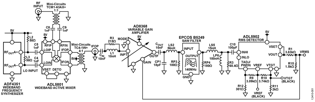
This circuit is a frequency selective, radio frequency (RF) detector that offers 90 dB of detection range from 35 MHz to 4.4 GHz. Unlike a standalone detector that does not discriminate between signals in the frequency spectrum, this circuit has the ability to focus on a narrow band of frequencies, providing enhanced performance over the specified range. The detector circuit is rms responding and stable vs. temperature and frequency, making it an attractive solution for applications that require precise frequency, selective RF power measurement. The circuit also demonstrates strong immunity to unwanted blockers. Figure 1 shows a simplified schematic of the circuit.

Circuit Description
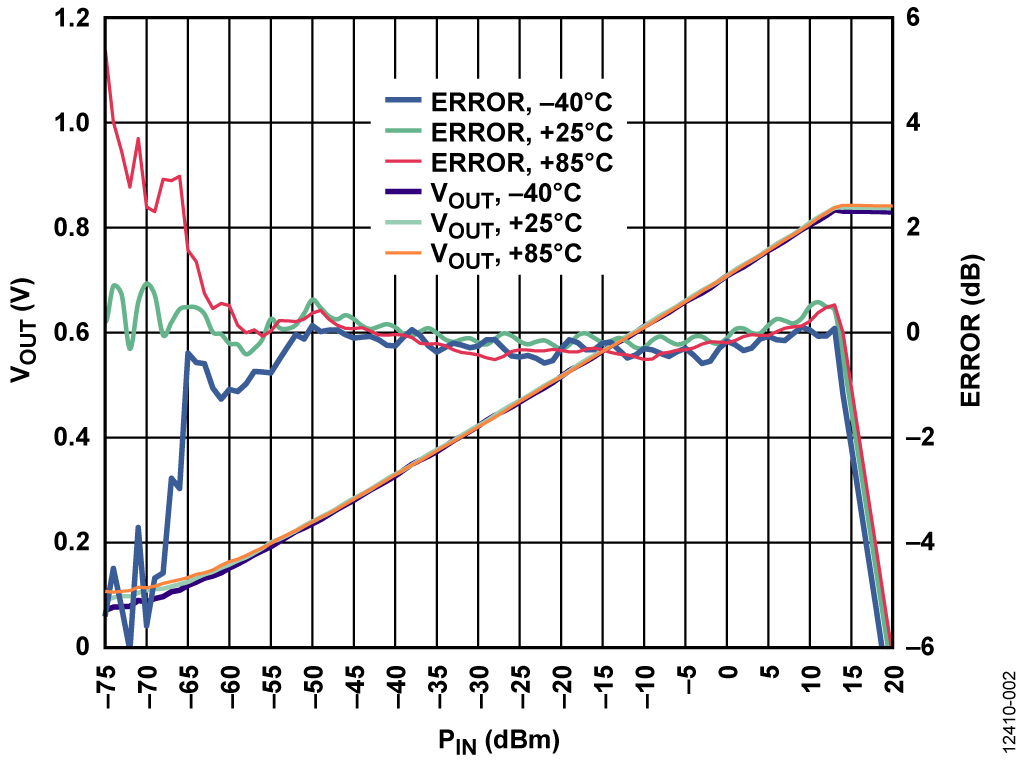
The detector circuit consists of an rms detector, a variable gain amplifier (VGA), a SAW filter, a mixer, and a frequency synthesizer that combine to provide a 90 dB detection range and excellent stability vs. frequency and temperature. Figure 2 shows the transfer function of the detector circuit when the input power is swept at 900 MHz. Optimum linearity is achieved using a four point calibration with calibration points at +13 dBm, −50 dBm, −65 dB, and −75 dBm. A two point calibration can also be used, but results in degraded linearity across the input power range.

The ADL5902 detector used in the circuit inherently provides 65 dB of detection range from 50 MHz to 9 GHz. The AD8368 VGA extends the upper and the lower end of the power range. The narrow-band SAW filter placed between the VGA and the detector maximizes the low end sensitivity by filtering noise from the VGA and the mixer. The Circuit Note CN-0340 describes this dynamic range extension mechanism in additional detail.
However, this range extension limits operation at the pass-band frequency range of the filter. Coupling the CN-0360 circuit with a wideband frequency translation network makes the combined circuit frequency-selective. In the circuit shown in Figure 1, the ADL5801 mixer is paired with the ADF4351 frequency synthesizer to translate input signals from 35 MHz to 4.4 GHz to 140 MHz, the pass-band frequency of the SAW filter. The Circuit Note CN-0239 describes the glueless broadband mixer and local oscillator interface used in the circuit.
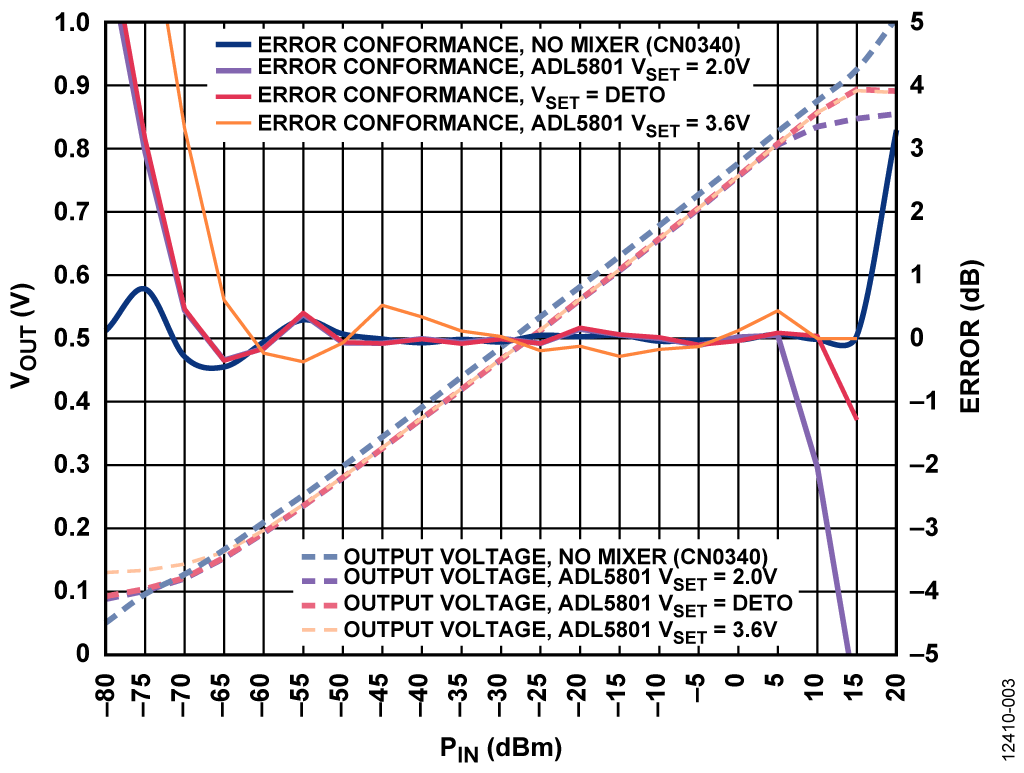
The circuit dynamic range was further enhanced by optimizing the mixer bias level using the VSET pin on the ADL5801 mixer. Typically, the ADL5801 mixer is operated at a VSET level of 3.6 V, resulting in high mixer bias and correspondingly high IP3. However, this operating point results in noise figure degradation, limiting input sensitivity. Operating the mixer at the minimum VSET level of 2.0 V improves mixer noise figure, but the P1dB of the mixer suffers as a result, limiting the dynamic range at the top end. The adaptive bias mechanism of the mixer is used to optimize the circuit detection range at both high and low power levels. By connecting the VSET pin to DETO, a pin routed to the internal power detector of the mixer, the device bias level is set adaptively based on signal conditions. This feature allows the mixer to provide high linearity and compression in the presence of large RF signals, and low noise figure in the presence of small RF signals. Implementing this feature improves the application sensitivity at lower input power levels, while also maintaining the dynamic range at the higher input power levels. Figure 3 shows the transfer function of the detector with various mixer bias levels.

Temperature Stability
Figure 2 shows the temperature stability of the detector vs. RF input power across the power spectrum. The accuracy over temperature was achieved using the temperature compensation feature on the ADL5902 rms detector to account for the temperature drift introduced into the system. Any temperature variation in the gain of the VGA and the mixer degrades the overall drift of the circuit one for one (that is, a 1 dB drift vs. temperature in the gain of the mixer degrades the overall temperature stability by 1 dB). In the case of the AD8368 VGA, Figure 5 in the AD8368 data sheet shows that the gain drift over temperature is approximately ±0.7 dB. Similarly, according to Figure 3 in the ADL5801 data sheet, the mixer drift over temperature is ±0.5 dB. Adjusting the voltage on the ADL5902 TADJ pin compensates for the combined temperature drift of the detector, VGA, and mixer. It was experimentally determined that a TADJ voltage of 0.6 V provides optimum temperature compensation at all RF input frequencies.
Frequency Stability
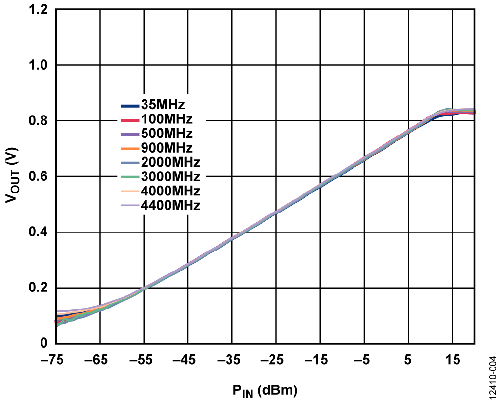
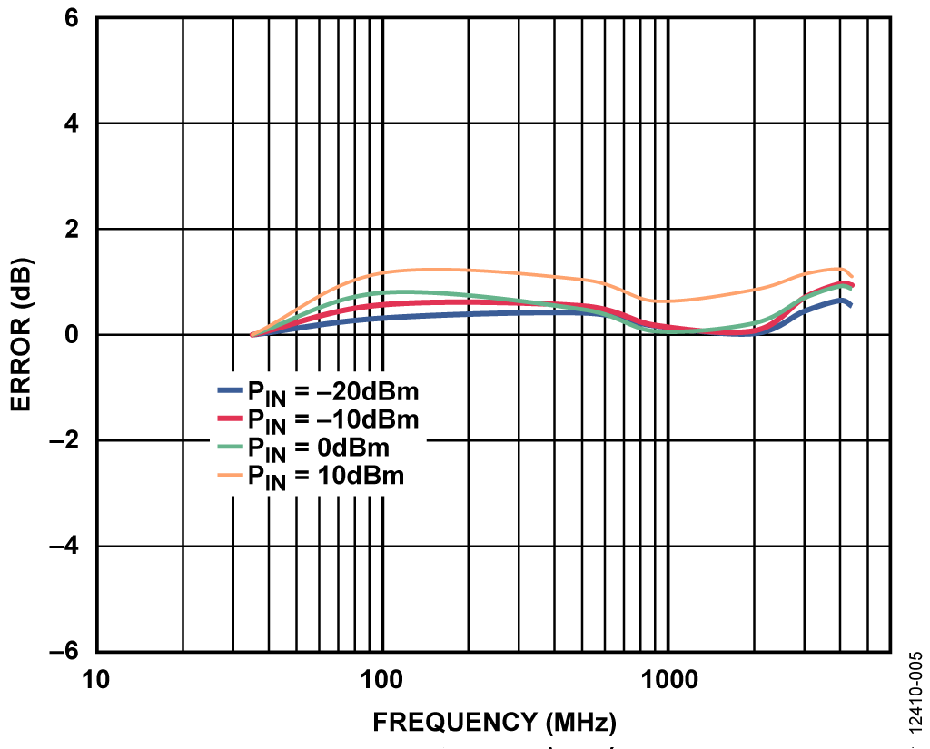
Figure 4 and Figure 5 display the circuit frequency flatness. The circuit exhibits approximately 1 dB flatness across the complete operating frequency range. Because the mixer downconverts input signals to 140 MHz, the gain variation introduced by the mixer dominates the frequency flatness profile.


Blocker Immunity
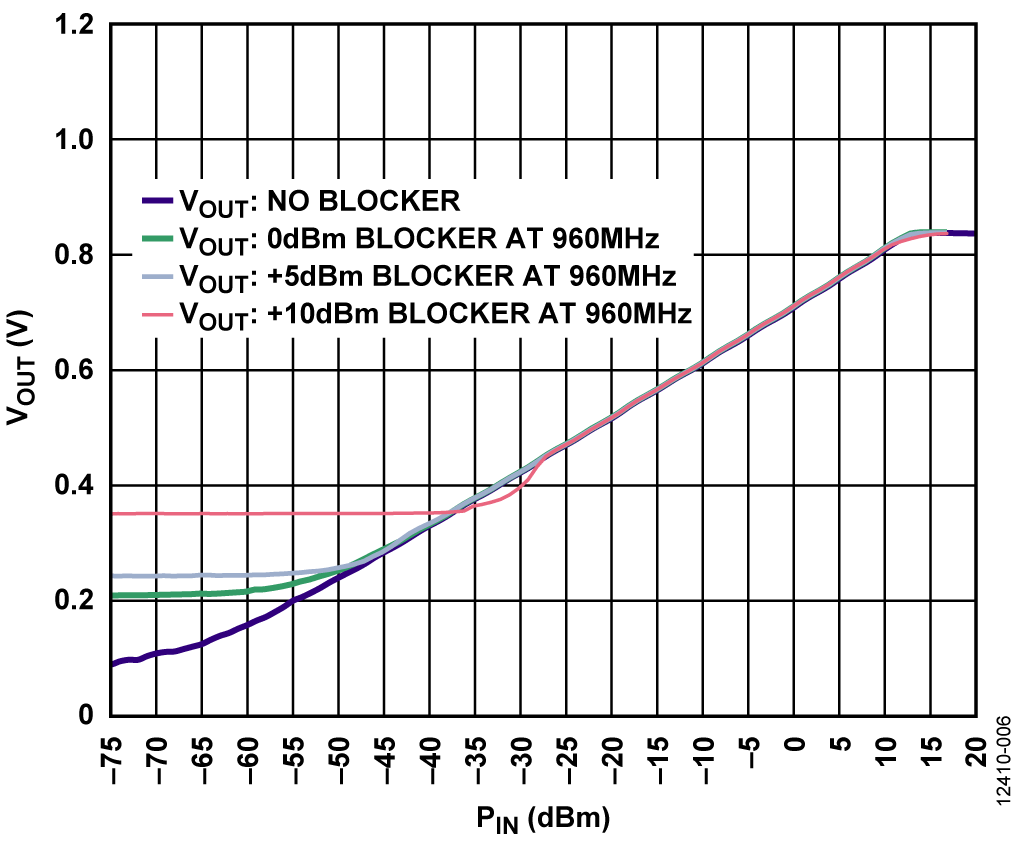
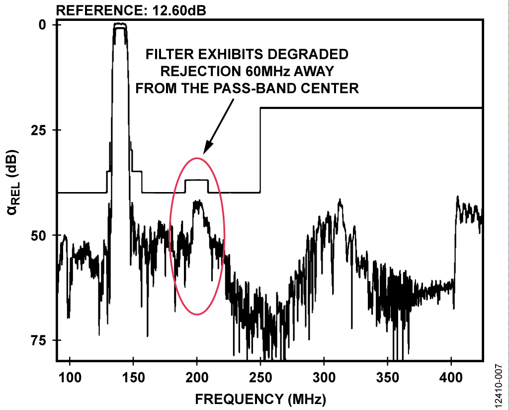
Figure 6 displays the performance of the circuit at 900 MHz when an unwanted blocking signal at 960 MHz is present. The blocking signal was placed 60 MHz away from carrier signal because the filter exhibits poor pass-band rejection at that frequency (see Figure 7), thus presenting the harshest test condition for the circuit. The blocking signal degrades the lower end sensitivity of the circuit for blocker input levels above −10 dBm; however, the circuit continues to maintain 65 dB of dynamic range for blocking signals of up to +5 dBm.


Common Variations
The frequency range of the circuit can be extended to 6 GHz by replacing the ADF4351 frequency synthesizer with a wider band discrete phase-locked loop (PLL), such as the ADF4155 or the ADF4156, and an external VCO. The intermediate frequency, filter bandwidth and insertion loss of the circuit can be modified by changing the SAW filter. Increasing the bandwidth and insertion loss of the filter increases the noise level, and consequently, lowers the dynamic range of the system. The integrated output noise level from the mixer, VGA, and filter must be 6 dB to10 dB lower than the nominal input sensitivity of the rms detector. ADIsimRF™ can be used to calculate the integrated noise of the circuit front end (mixer, VGA, and filter). The circuit output voltage can be digitized by pairing the circuit with an analog-to-digital converter (ADC) such as the AD7091 or the AD7466. See the Circuit Note CN-0178 for more details.
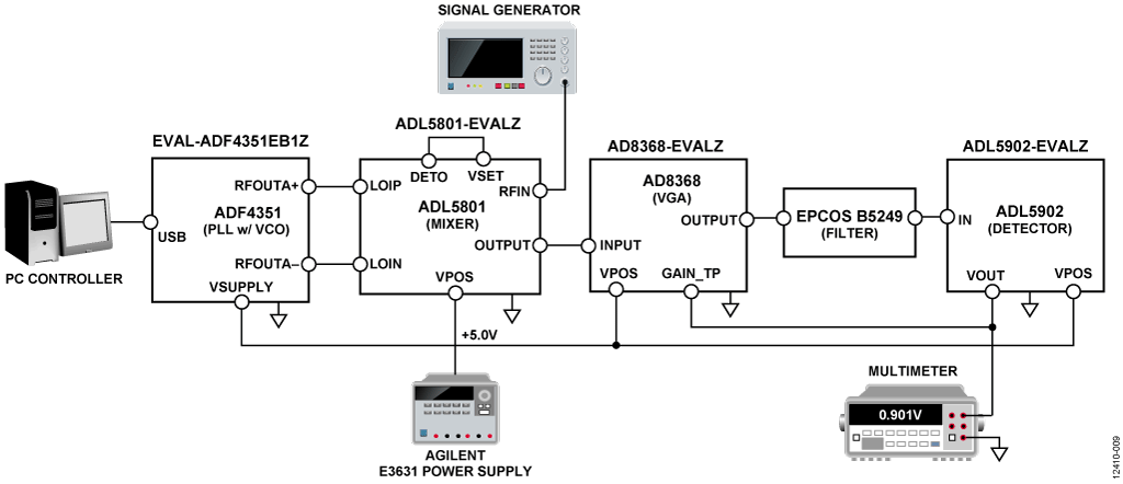
Circuit Evaluation & Test
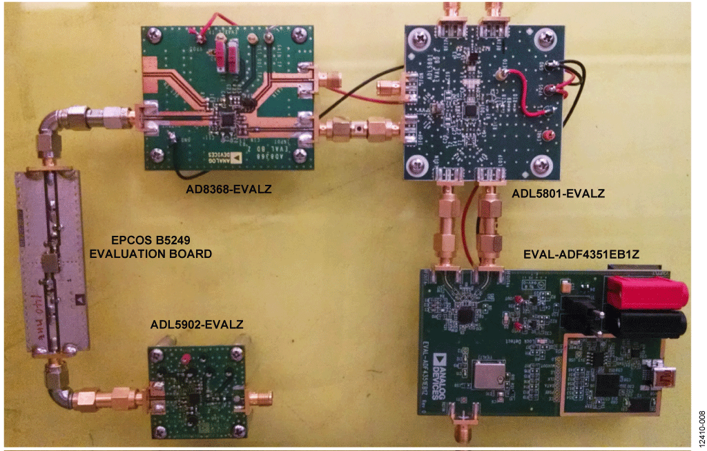
The circuit was implemented using the standard evaluation boards for the ADL5902 (ADL5902-EVALZ), the AD8368 (AD8368-EVALZ), the ADF4351 (EVAL-ADF4351EB1Z), the ADL5801 (ADL5801-EVALZ), and a filter evaluation board populated with the EPCOS B5249 SAW filter. Because all the evaluation boards have 50 Ω interfaces, they were connected directly using barrel SMA connectors. Test clips were used to connect the signal connection from the output of the ADL5902 detector back to the gain control input of the AD8368, and to connect the VSET and DET0 pins to configure the adaptive bias control on the ADL5801. The resistor divider that is required to scale down the output voltage of the ADL5902 detector was implemented by placing surface mount resistors on the R1 (3.83 kΩ) and R15 (1.5 kΩ) pads on the ADL5902 evaluation board. The TADJ voltage that optimizes the temperature stability of the circuit at 140 MHz was set by the R9/R12 resistor divider, which is derived from the 2.3 V on-chip voltage reference. To set the TADJ voltage to the recommended 0.6 V level, change R9 to 850 Ω (R12 keeps its existing value of 301 Ω).
Figure 8 shows the assembled application circuit, and Figure 9 shows a block diagram of the test setup.


Equipment Needed
The following is a list of equipment used to evaluate the circuit.
- Windows XP, Windows Vista (32-bit), or Windows 7 (32-bit) PC with USB port
- The ADL5902-EVALZ, AD8368-EVALZ, EVAL-ADF4351EB1Z, and ADL5801-EVALZ evaluation boards
- The EPCOS B5249 evaluation board
- An RF signal generator
- A digital multimeter
- A power supply
The ADF4351 control software was used to program the LO frequency required to downconvert the input signal to an intermediate frequency of 140 MHz. The rms output voltage of the circuit was then measured as a function of increasing input power levels to determine the transfer function and error conformance profile of the circuit.
To test the immunity of the circuit to blocker signals, the circuit was driven with a signal generator emulating the blocker combined with the primary signal generator emulating the channel of interest. The circuit performance was evaluated in response to increasing levels of the blocker signal.