CN0147


Overview
Design Resources
Evaluation Hardware
Part Numbers with "Z" indicate RoHS Compliance. Boards checked are needed to evaluate this circuit.
- EVAL-ADF4350EB1Z ($224.70) ADF4350 evaluation board used to evaluate this circuit. Please see "Circuit Evaluation & Test" section for set up information.
Device Drivers
Software such as C code and/or FPGA code, used to communicate with component's digital interface.
ADF4350 GitHub Linux Driver Source Code
ADF4350 GitHub no-OS Driver Source Code
ADF4350 IIO Wideband Synthesizer GitHub Linux Driver Source Code
Features & Benefits
- Frequency range from 140 MHz to 4.4 GHz
- Ultralow noise regulators for optimal system phase noise
Product Categories
Markets and Technologies
Parts Used
Documentation & Resources
Circuit Function & Benefits
This circuit uses low noise, low dropout (LDO) linear regulators to supply power to a wideband integrated PLL and VCO. Wideband voltage controlled oscillators (VCOs) may have increased sensitivity to power supply noise, hence, ultralow noise regulators are recommended for best performance.
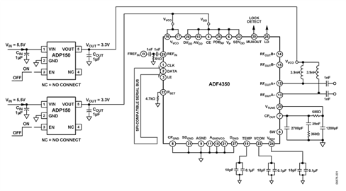
The circuit shown in Figure 1 utilizes the ADF4350, a fully integrated fractional-N PLL and VCO that can generate frequencies from 137.5 MHz to 4400 MHz. The ADF4350 is powered from the ultralow noise 3.3 V ADP150 regulator for optimal LO phase noise performance.


The lower integrated rms noise of the ADP150 LDO of only 9 μV rms (10 Hz to 100 kHz) helps to minimize VCO phase noise and reduce the impact of VCO pushing (the VCO equivalent of power supply rejection).
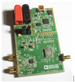
Figure 2 shows a photo of the evaluation board, which uses the ADP150 LDOs to power the ADF4350. The ADP150 represents the industry’s lowest noise LDO in the smallest package at the lowest cost. It is available in a 4-ball, 0.8 mm × 0.8 mm, 0.4 mm pitch WLCSP or a convenient 5-lead TSOT package. Adding the ADP150’s to the design, therefore, has minimal impact on system cost and board area while providing a significant improvement in phase noise.


Circuit Description
The ADF4350 is a wideband PLL and VCO consisting of three separate multiband VCOs. Each VCO covers a range of approximately 700 MHz (with some overlap between VCOs). Lower frequencies are generated by output dividers.
VCO pushing is measured by applying a steady dc tuning voltage to the ADF4350 VTUNE pin, varying the power supply voltage, and measuring the frequency change. The pushing figure (P) equals the frequency delta divided by the voltage delta, as shown in Table 1.
| VCO Frequency (MHz) |
VTUNE (V) |
VCO Pushing (MHz/V) |
| 2200 |
2.5 |
0.73 |
| 3300 |
2.5 |
1.79 |
| 4400 |
2.5 |
5.99 |
In a PLL system, higher VCO pushing means that power supply noise will degrade the VCO phase noise. If VCO pushing is low, then power supply noise will not significantly degrade phase noise. However, for high VCO pushing, noisy power supplies will have a measurable impact on phase noise performance.
Experiments showed pushing to be at its maximum at 4.4 GHz VCO output frequency, so the comparison of VCO performance with different regulators was made at this frequency. Rev. A evaluation boards of the ADF4350 used the ADP3334 LDO regulator. The integrated rms noise of this regulator is 27 μV (integrated from 10 Hz to 100 kHz). This compares to 9 μV for the ADP150, which is used on the EVAL-ADF4350EB1Z, Rev B. In order to measure the impact of the power supply noise, a narrow PLL loop bandwidth (10 kHz) was used to facilitate greater examination of VCO phase noise. A diagram of this setup is shown in Figure 3. A more detailed examination of the output noise density with frequency is available from the data sheets of both the ADP3334 and ADP150.


Figure 4 shows that the noise spectral density of the ADP3334 regulator is 150 nV/√Hz at 100 kHz offset. The same plot for the ADP150 (Figure 5) shows 25 nV /√Hz.


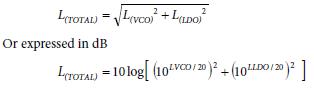
The formula for calculating the degradation in phase noise due to the power supply noise is as follows:

Where L(LDO) is the noise contribution from the regulator to the VCO phase noise (in dBc/Hz), at an offset fm; P is the VCO pushing figure in Hz/V; Sfm; is the noise spectral density at a given frequency offset in V/√Hz; and fm; is the frequency offset at which the noise spectral density is measured in Hz.


The noise contribution from the supply is then rss summed with the noise contribution of the VCO (itself measured with a very low noise supply) to give the total noise at the VCO output with a given regulator.
These noise performances are rss summed together to give the expected VCO phase noise:
In this example, a 100 kHz noise spectral density offset is chosen, a 6 MHz/V pushing figure is used, and −110 dBc/Hz is taken as the VCO noise with an ideal supply.
Using a dedicated signal source analyzer (like Rohde & Schwarz FSUP), the VCO phase noise is compared. At 100 kHz offset the ADP3334 delivers −102.6 dBc/Hz (Figure 6), and in the same configuration the ADP150 measures −108.5 dBc/Hz (Figure 7).
| ADP3334 |
ADP150 |
|
| Noise contribution from regulartor (nV/√Hz) |
150 |
25 |
| Noise contribution from regulartor (dBc/Hz) |
–104 |
–119.5 |
| Total calculated noise at VCO output (dBc/Hz) |
–103 |
–109.5 |
| Measured VCO nose at 100 kHz offset (dBc/Hz) |
–102.6 |
–108.5 |

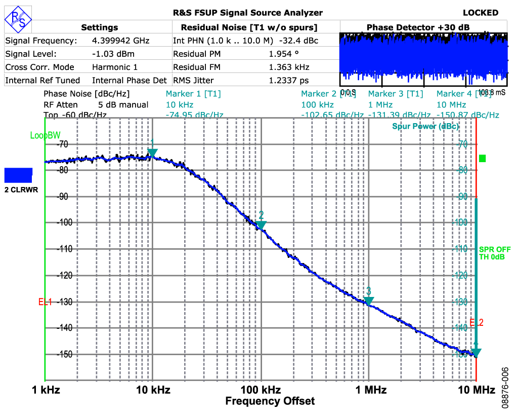

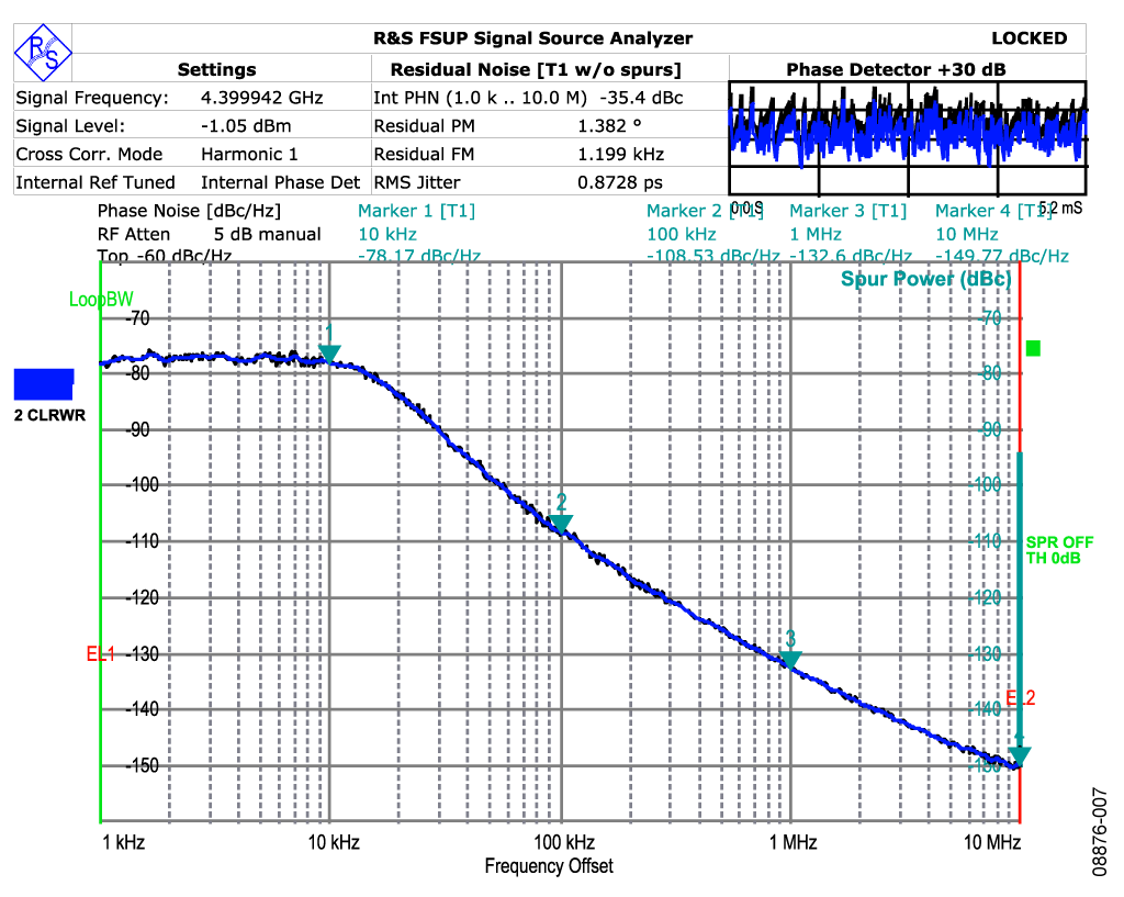
The integrated phase noise improves from 1.95° to 1.4° rms also. The measured results correlate very closely with the calculations and clearly show the benefit of using the ADP150 with the ADF4350.
A complete design support package for this circuit note can be found at http://www.analog.com/CN0147-DesignSupport.
Common Variations
Additional regulators can be added for greater isolation between power supplies, if desired. Also, one ADF150 regulator can be used to power the entire ADF4350 part. However, care needs to be taken in this case to ensure the maximum rated current of the single ADP150 regulator is not exceeded. This is possible if the lowest output power setting on the ADF4350 is selected.
Circuit Evaluation & Test
This circuit note, CN-0147, uses the EVAL-ADF4350EB1Z board for evaluation of the described circuit, allowing for quick setup and evaluation. The EVAL-ADF4350EB1Z board uses the standard ADF4350 programming software, contained on the CD that accompanies the evaluation board.
Equipment Needed
Windows® XP, Windows, Vista (32-bit), or Windows 7 (32-bit) PC with USB Port, the ADF4350EB1Z, the ADF4350 programming software, 5.5 V power supply, and a spectrum analyzer such as a Rhode and Schwartz FSUP26. See this circuit note CN-0147 and UG-109 user guide for evaluation board EVAL-ADF435EB1Z and the ADF4350 data sheet.
Getting Started
This circuit note, CN-0147, contains a description of the circuit, the schematic, and a block diagram of the test setup. The ser guide, UG-109, details the installation and use of the EVAL-ADF4350 evaluation software. UG-109 also contains board setup instructions and the board schematic, layout, and bill of materials.
Functional Block Diagram
This circuit note, CN-0147, contains the function block diagram of the described test setup in Figure 3.
Setup and Test
After setting up the equipment, standard RF test methods should be used to measure the spectral purity of the output signal.