CN0204


Overview
Design Resources
Design & Integration File
- Schematic
- Bill of Materials
- Gerber Files
- PADS Files
- Assembly Drawing
Evaluation Hardware
Part Numbers with "Z" indicate RoHS Compliance. Boards checked are needed to evaluate this circuit.
- EVAL-CN0204-SDPZ ($69.55) Flexible, High Voltage, High Accuracy, Low Drift PLC/DCS Analog Output Module
- EVAL-SDP-CB1Z ($116.52) Eval Control Board SDP
Device Drivers
Software such as C code and/or FPGA code, used to communicate with component's digital interface.
AD5760, AD578x, AD579x IIO DAC GitHub Linux Driver Source Code
Features & Benefits
- High voltage, up to 44V
- Programmable analog output
- Galvanic isolation from rest of system
- Ideal for PLC and DCS modules
Product Categories
Markets and Technologies
Parts Used
Documentation & Resources
-
CN0204 Software User Guide10/18/2018WIKI
-
The Data Conversion Handbook, 20051/2/2005
-
MT-101: Decoupling Techniques2/14/2015PDF954 kB
-
MT-031: Grounding Data Converters and Solving the Mystery of "AGND" and "DGND"3/20/2009PDF144 kB
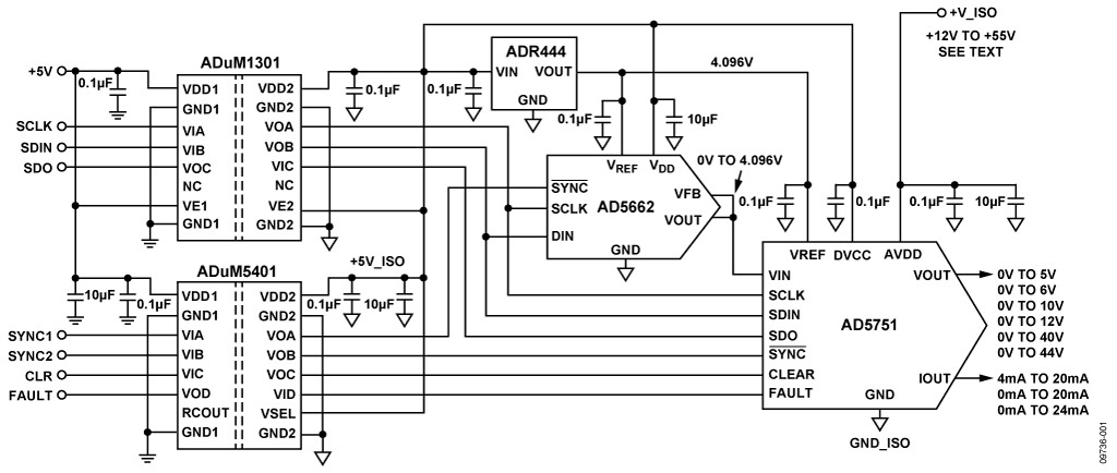
Circuit Function & Benefits
The circuit, shown in Figure 1, provides a full function, high voltage (up to 44 V), flexible, programmable analog output solution that meets most requirements for programmable logic controller (PLC) and distributed control system (DCS) applications.
The AD5662 low power (0.75 mW typical @ 5 V), rail-to-rail output, 16-bit nanoDAC® device and the AD5751 industrial current/voltage output driver are well matched with respect to input and output voltage ranges, as well as reference voltage requirements.
The ADR444, with low drift (3 ppm/℃ maximum for B grade), high initial accuracy (0.04% maximum for B grade), and low noise (1.8 μV p-p typical, 0.1 Hz to 10 Hz), provides the reference voltage for both the AD5751 and AD5662 and guarantees ultralow noise, high accuracy, and low temperature drift for the circuit. This circuit provides all the typical voltage and current output ranges with 16-bit resolution and no missing codes, 0.05% linearity, and less than 0.2% total output error.
The ADuM1301 and ADuM5401 provide all the necessary signal isolation between the microcontroller and the analog signal chain. The ADuM5401 also provides isolated 5 V power. The circuit also contains key features for industrial applications, such as on-chip output fault detection, CRC checking to prevent packet error (PEC), and flexible power-up options, making it an ideal choice for robust industrial control systems. No external precision resistors or calibration routines are needed to maintain consistent performance in mass production, thereby making it ideal for PLC or DCS modules.

Circuit Description
The AD5751 is a single channel, low cost, precision voltage/current output driver developed to meet the requirements of industrial process control applications. The AD5751 is specified to operate with a power supply range from 10.8 V to 55 V, and the voltage output can be up to 44 V. The voltage output range can be programmed for the standard output ranges and 20% overrange settings for PLC and DCS applications: 0 V to 5 V, 0 V to 10 V, 0 V to 6 V, 0 V to 12 V. In addition, two high voltage output ranges are also provided: 0 V to 40 V and 0 V to 44 V.
The current output, which is provided on a separate pin, can be programmed for the standard ranges of 4 mA to 20 mA, 0 mA to 20 mA, 0 mA to 24 mA. There is also a 2% overrange setting which provides 3.92 mA to 20.4 mA, 0 mA to 20.4 mA, and 0 mA to 24.5 mA. The voltage and current output pins can be tied together to configure the end system as a single-channel output if desired.
The AD5662 is a single channel, low cost, low power, rail-to-rail voltage buffered output nanoDAC device. The AD5662 guarantees ±1 LSB DNL under a wide range of reference voltages that can vary from 0.75 V to the VDD supply. In the circuit of Figure 1, the AD5751 and AD5662 operate from a common reference source of 4.096 V, provided by the ADR444. The whole system will benefit from the ultralow noise and low temperature coefficient of the ADR444. The ADR44x family of references are ideal for driving either the reference or the power input of converters because they can source and sink current. The AD5662 also incorporates a power-on reset circuit to ensure that the DAC output powers up to either midscale or zero and remains there until a valid write takes place.
The ADuM1301 is a triple channel digital isolator. The ADuM5401 is a quad channel digital isolator with isoPower® integrated, isolated, dc-to-dc converter. They are both based on the iCoupler® technology. They are used to provide isolation between the signal chain and the system microcontroller, with an isolation rating of 2.5 kV rms. The ADuM5401 provides an isolated 5 V power supply for all the circuit in the secondary side.
The digital power and analog power should be separated and connected with a ferrite bead. Each power is well decoupled by a 10 μF paralleled with a 0.1 μF ceramic capacitor. See the schematics in the CN0204 Design Support package for more details.
Devices for PLC and DCS applications generally need ESD protection and overvoltage protection much higher than the formal recommended specifications. The AD5751 has integrated ESD protection diodes internal to each pin that can prevent damage from transients. However, the industrial control environment can subject I/O circuits to much higher transients. External 64 V, 1500 W transient voltage suppressors (TVS); a 50 mA, 30 V PolySwitch; and power Schottky diodes are built into the EVAL-CN0204-SDPZ circuit board to provide higher voltage ESD protection, 50 mA overcurrent, and 64 V overvoltage protection. The optional external protection circuits are not shown in the simplified schematic of Figure 1 but can be found in the detailed schematic (EVAL-CN0204- SDPZ-SCH pdf file) in the CN0204 Design Support package: www.analog.com/CN0204-DesignSupport.
The circuit must be constructed on a multilayer PC board with a large area ground plane. Proper layout, grounding, and decoupling techniques must be used to achieve optimum performance (see Tutorial MT-031, Grounding Data Convertersand Solving the Mystery of "AGND" and "DGND," and Tutorial MT-101, Decoupling Techniques).
Measurements
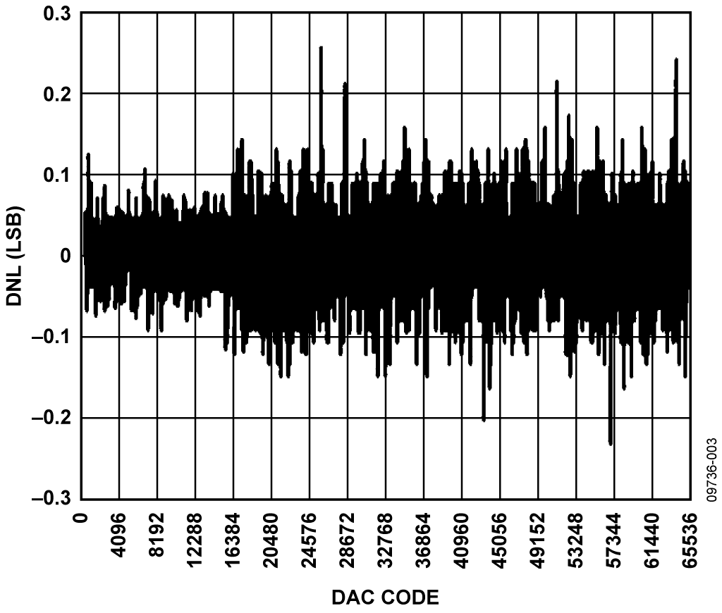
Integral nonlinearity (INL), differential nonlinearity (DNL), and output error are the most important specifications for PLC, DCS, and other process control systems. The AD5751 has highly flexible and configurable output ranges that can be tailored to meet the needs of the application. Measurements of INL, DNL, and output error for the circuit are shown in Figure 2, Figure 3, and Figure 4, respectively. This data was taken at 25°C in the voltage output mode using the internal current sense resistor. The AD5751 range was set for 0 V to 5 V. The test results for all the other ranges are listed in Table 1.
The test results shown in Table 1 were made at 25°C using the EVAL-CN0204-SDPZ board powered by an Agilent E3631A dc supply and measured with an Agilent 34401A digital multimeter.
Note that the output ranges 0 mA to 20.4 mA and 0 mA to 24.5 mA are both designed to be trimmed by the customer to precisely match the 0 mA to 20 mA and 0 mA to 24 mA ranges. The 1.70% FSR output error measurement in the 0 mA to 20.4 mA range includes the gain error, which can be removed by customer calibration.


| Range | Current Sense Resistor | INL (LSB) | Linearity (%FSR) | Output Error (%FSR) |
| 0V to 5V | Don't Care | 10.8 | 0.017 | 00.09 |
| 0V to 10V | Don't Care | 9.9 | 0.015 | 0.08 |
| 0V to 6V | Don't Care | 10.5 | 0.016 | 0.09 |
| 0V to 12V | Don't Care | 9.2 | 0.014 | 0.08 |
| 0V to 40V | Don't Care | 10.1 | 0.015 | 0.06 |
| 0V to 44V | Don't Care | 9.5 | 0.015 | 0.020 |
| 4 mA to 20 mA | Internal | 8.5 | 0.016 | 0.04 |
| 4 mA to 20 mA | External | 8.4 | 0.013 | 0.04 |
| 0 mA to 20 mA | Internal | 9.8 | 0.015 | 0.05 |
| 0 mA to 20 mA | External | 8.9 | 0.014 | 0.05 |
| 0 mA to 24 mA | Internal | 8.4 | 0.013 | 0.05 |
| 0 mA to 24 mA | External | 12.0 | 0.018 | 0.05 |
| 3.9 mA to 20.4 mA | Internal | 11.8 | 0.053 | 0.80 |
| 0 mA to 20.4 mA | Internal | 9.4 | 0.014 | 1.70 |
| 0 mA to 24.5 mA | Internal | 12.4 | 0.019 | 1.50 |


Common Variations
This circuit describes one implementation of a family of driver and DAC products, from which various devices can be selected to achieve desired performance. Resolution of 12 bits to 16 bits with 0.1% accuracy are typical requirements for PLC and DCS applications. For applications not requiring 16-bit resolution, the AD5620 (12-bit) and AD5640 (14-bit) are available, and have internal references.
For multichannel applications, the AD5623R (12-bit), AD5643R (14-bit), and AD5663R (16-bit) are dual nanoDAC devices, and the AD5624R (12-bit), AD5644R (14-bit), and AD5664R (16-bit) are quad nanoDAC devices.
The AD5750-1 and AD5750 are both bipolar analog output drivers and can supply ±10 V and ±20 mA.
Circuit Evaluation & Test
Equipment Needed (Equivalents Can Be Substituted)
- System Demonstration Platform (EVAL-SDP-CB1Z)
- CN-0204 Circuit Evaluation Board (EVAL-CN0204-SDPZ)
- CN-0204 Evaluation Software
- Software for controlling external test measurement equipment (not included on CD)
- Agilent 34401A, 6.5 Digit Digital Multimeter
- Agilent E3631A 0 V to 6 V/5 A; ±25 V/1 A triple output dc power supply
- PC (Windows® 2000 or Windows XP) with USB interface
- National Instruments GPIB to USB-B interface and cable
Getting Started
Load the evaluation software by placing the CN0204 Evaluation Software disc in the CD drive of the PC. Using "My Computer," locate the drive that contains the evaluation software disc and open the Readme file. Follow the instructions contained in the Readme file for installing and using the evaluation software.
Functional Block Diagram
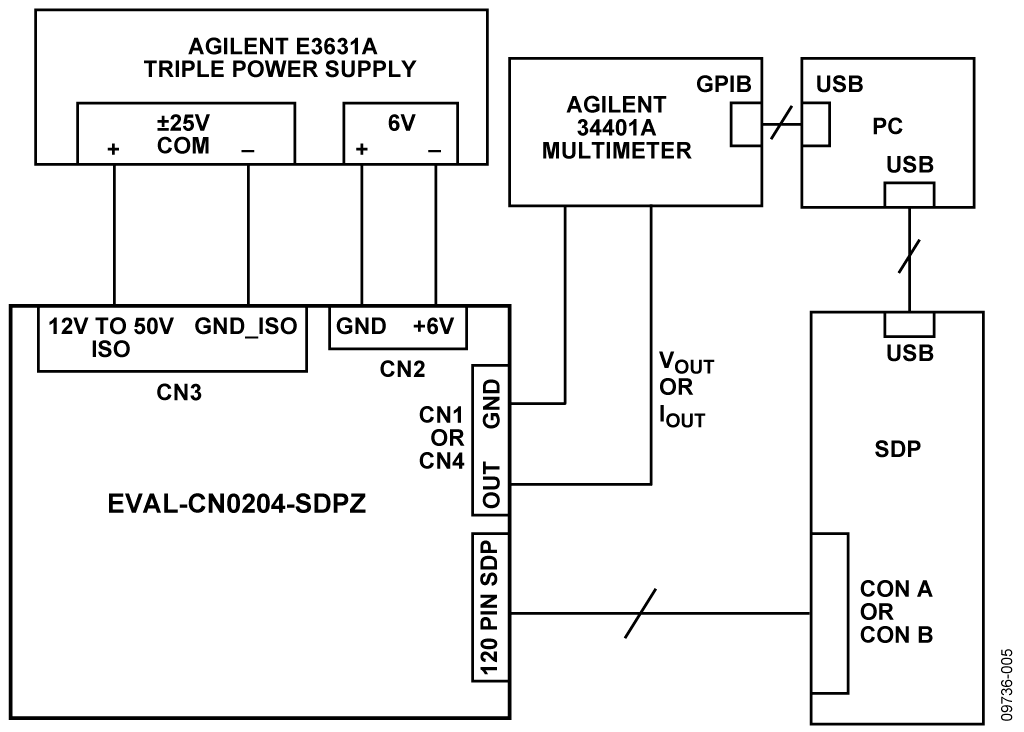
Figure 5 shows a functional block diagram of the test setup. The pdf file “EVAL-CN0204-SDPZ-SCH” contains the detailed circuit schematics for the CN0204 evaluation board. This file is contained in the CN-0204 Design Support Package: www.analog.com/CN0204-DesignSupport.
Setup
Connect the 120-pin connector on the EVAL-CN0204-SDPZ circuit board to the connector marked “CON A” or “CON B” on the EVAL-SDP-CB1Z evaluation (SDP) board. Nylon hardware should be used to firmly secure the two boards, using the holes provided at the ends of the 120-pin connectors. After setting the dc output supply to +25 V, −25 V and +6 V output, turn the power supply off.
The Agilent E3631A supply has ±25 V/1 A and 6 V/5 A output channels. The ±25 V/1 A and 6 V/5 A are isolated with respect to each other. Therefore, the ±25 V/1 A can be used to provide the +50 V power supply to the circuit. There must be no external connection between the “−” terminal of the 6 V/5 A supply and the “COM” terminal of the ±25 V/1 A supply.
With power to the supply off, connect a +25 V power supply to the pin of CN3 marked “12~50VIN,” and the −25 V power supply to the pin of CN3 marked “GND_ISO.” Leave the “COM” of ±25 V/1 A unconnected. Connect +6 V to CN2 the same way. Turn on the power supply and then connect the USB cable with the SDP board to the USB port on the PC. Note: Do not connect the USB cable to the mini USB connector on the SDP board before turning on the dc power supply for the EVAL-CN0204-SDPZ.

| Jumper | Descriptions | Setting | Function |
| JP1 | Sets the address of AD5751 | Shorting Pin1 with Pin2 | Address of AD5751 : b'001 |
| Shorting Pin3 with Pin2 | Address of AAD5751 : b'000 | ||
| JP2 | Sets the external compensation capacitor | Shorting | Adding 1 nF Compensation Capacitor |
| Opening | Removing 1 nF Compensation Capacitor | ||
| JP3 | VSENSE+ Setting | Shorting | Shorting VSENSE+ with VOUT internally |
| Opening | VSENSE+ has no connection with VOUT internally | ||
| JP4 | Sets the CLEAR Mode for AD5751 | Shorting | Clears to midscale |
| Opening | Clears to zero scale | ||
| JP5 | Shorts the VOUT and IOUT pins | Shorting | Shorts VOUT and IOUT together |
| Opening | VOUT and IOUT have no connection internally |
Test
After setting up the test equipment, connect the pin of CN4 marked “VOUT” or the pin of CN1 marked “IOUT” to the input of the Agilent 34401A. Make sure that the cable connection on the front panel of the Agilent 34401A is correct, depending on the different input signal type (current or voltage). Testing the INL, DNL, and total error will take a considerable amount of time because all of the AD5662 16-bit DAC levels must be set and measured by the 34401A.
The software provided on the CD allows the DAC codes to be set by the PC. An automatic test program is necessary to step through the codes and analyze the data. This is not provided on the CD but must be implemented by the customer to correspond to the requirements of the particular multimeter used in the test setup.
In the test configuration shown in Figure 5, the GPIB output of the 34401A multimeter interfaces to a second USB port on the PC using the National Instruments GPIB to USB-B interface and cable. This allows the multimeter readings corresponding to each code to be loaded into an Excel spreadsheet on the PC. The data is then analyzed for INL, DNL, and total error using industry-standard definitions.
For more details on the definitions and how to calculate the INL, DNL, and total error from the measured data, see the "TERMINOLOGY" section of the AD5662 data sheet and also the following reference: Data Conversion Handbook, "Testing Data Converters", Chapter 5, Analog Devices.