CN0187


Overview
Design Resources
Design & Integration File
- Schematic
- Bill of Materials
- Gerber Files
- PADS Files
- Assembly Drawing
Evaluation Hardware
Part Numbers with "Z" indicate RoHS Compliance. Boards checked are needed to evaluate this circuit.
- EVAL-CFTL-6V-PWRZ ($20.01) Wall Power Supply for Eval Board
- EVAL-CN0187-SDPZ ($58.85) Crest Factor, Peak, and RMS RF Power Measurement Circuit Optimized for High Speed, Low Power, and Single 3.3 V Supply
- EVAL-SDP-CB1Z ($116.52) Eval Control Board SDP
Device Drivers
Software such as C code and/or FPGA code, used to communicate with component's digital interface.
Features & Benefits
- Measures crest factor, peak power, and RMS power
- Wide frequency range from 450 MHz to 6 GHz
- Optimized for low power RF monitoring
Product Categories
Markets and Technologies
Parts Used
Documentation & Resources
-
CN0187 Software User Guide10/18/2018WIKI
-
MT-081: RMS-to-DC Converters2/14/2015PDF230 K
-
High Frequency Log Amps2/14/2015PDF144 kB
-
MT-101: Decoupling Techniques2/14/2015PDF954 kB
-
MT-073: High Speed Variable Gain Amplifiers2/14/2015PDF177 kB
-
MT-031: Grounding Data Converters and Solving the Mystery of "AGND" and "DGND"3/20/2009PDF144 kB
-
Design and Operation of Automatic Gain Control Loops for Receivers in Modern Communication Systems10/10/2003PDF129 kB
Circuit Function & Benefits
The circuit shown in Figure 1 measures peak and rms power at any RF frequency from 450 MHz to 6 GHz over a range of approximately 45 dB. The measurement results are converted to differential signals in order to eliminate noise and are provided as digital codes at the output of a 12-bit SAR ADC with serial interface and integrated reference. A simple twopoint calibration is performed in the digital domain.
The ADL5502 is a mean-responding (true rms) power detector in combination with an envelope detector to accurately determine the crest factor (CF) of a modulated signal. It can be used in high frequency receiver and transmitter signal chains from 450 MHz to 6 GHz with envelope bandwidths over 10 MHz. The peak-hold function allows the capture of short peaks in the envelope with lower sampling rate ADCs. Total current consumption is only 3 mA @ 3 V.
The ADA4891-4 is a high speed, quad, CMOS amplifier that offers high performance at a low cost. Current consumption is only 4.4 mA/amplifier at 3 V. The amplifier features true singlesupply capability, with an input voltage range that extends 300 mV below the negative rail. The rail-to-rail output stage enables the output to swing to within 50 mV of each rail, ensuring maximum dynamic range. Low distortion and fast settling time makes it ideal for this application.
The AD7266 is a dual, 12-bit, high speed, low power, successive approximation ADC that operates from a single 2.7 V to 5.25 V power supply and features sampling rates up to 2 MSPS. The device contains two ADCs, each preceded by a 3-channel multiplexer, and a low noise, wide bandwidth track-and-hold amplifier that can handle input frequencies in excess of 30 MHz. Current consumption is only 3 mA at 3 V. It also contains an internal 2.5 V reference.
The circuit operates on a single +3.3 V supply from the ADP121, a low quiescent current, low dropout, linear regulator that operates from 2.3 V to 5.5 V and provides up to 150 mA of output current. The low 135 mV dropout voltage at 150 mA load improves efficiency and allows operation over a wide input voltage range. The low 30 μA of quiescent current at full load makes the ADP121 ideal for battery-operated portable equipment.
The ADP121 is available in output voltages ranging from 1.2 V to 3.3 V. The parts are optimized for stable operation with small 1 μF ceramic output capacitors. The ADP121 delivers good transient performance with minimal board area. Short-circuit protection and thermal overload protection circuits prevent damage in adverse conditions. The ADP121 is available in tiny 5-lead TSOT and 4-ball, 0.4 mm pitch halidefree WLCSP packages and utilizes the smallest footprint solution to meet a variety of portable applications.


Circuit Description
The RF signal being measured is applied to the ADL5502. A single 75 Ω termination resistor at the RF input in parallel with the input impedance of the ADL5502 provides a broadband match of 50 Ω. More precise resistive or reactive matches can be applied for narrow frequency band use (see the RF Input Interfacing section of the ADL5502 data sheet).
The internal filter capacitor of the ADL5502 provides averaging in the square domain but leaves some residual ac on the output. Signals with high peak-to-average ratios, such as W-CDMA or CDMA2000, can produce ac residual levels on the ADL5502 VRMS dc output. To reduce the effects of these low frequency components in the waveforms, some additional filtering is required. The internal square-domain filter capacitance of the ADL5502 can be augmented by connecting a CFLTR capacitor between Pin 1 (FLTR) and Pin 2 (VPOS). The ac residual can be reduced further by adding capacitance to the VRMS output. The combination of the internal 100 Ω output resistance and the added output capacitance produces a low-pass filter to reduce output ripple of the VRMS output (see the Selecting the Square-Domain Filter and Output Low-Pass Filter section of the ADL5502 data sheet for more details).
To measure the peak of a waveform, the control line (CNTL) must be temporally set to a logic high (reset mode for >1 μs) and then set back to a logic low (peak-hold mode). This allows the ADL5502 to be initialized to a known state. When setting the device to measure peak, peak-hold mode should be toggled for a period in which the input rms power and crest factor (CF) is not likely to change.
If the ADL5502 is in peak-hold mode and the CF changes from high to low or the input power changes from high to low, a faulty peak measurement is reported. The ADL5502 simply keeps reporting the highest peak that occurred when the peakhold mode was activated and the input power or the CF was high. Unless CNTL is reset, the PEAK output does not reflect the new peak in the signal.
The ADL5502 is capable of sourcing a VRMS output current of approximately 3 mA. The output current is sourced through the on-chip, 100 Ω series resistor; therefore, any load resistor forms a voltage divider with this on-chip resistance. It is recommended that the ADL5502 VRMS output drive high resistive loads to preserve output swing. If an application requires driving a low resistance load (as well as in cases where increasing the nominal conversion gain is desired), a buffering circuit is necessary.
The PEAK output is designed to drive 2 pF loads. It is recommended that the ADL5502 PEAK output drive low capacitive loads to achieve a full output response time. The effects of larger capacitive loads are particularly visible when tracking envelopes during the falling transitions. When the envelope is in a fall transition, the load capacitor discharges through the on-chip load resistance of 1.9 kΩ. If the larger capacitive load is unavoidable, the additional capacitance can be counteracted by putting a shunt resistor to ground on the PEAK output to allow for fast discharge. Such a shunt resistor also makes the ADL5502 run higher current, and it should not be lower than 500 Ω.
Typical measured performance characteristics of the circuit are presented in Figure 2 through Figure 5.


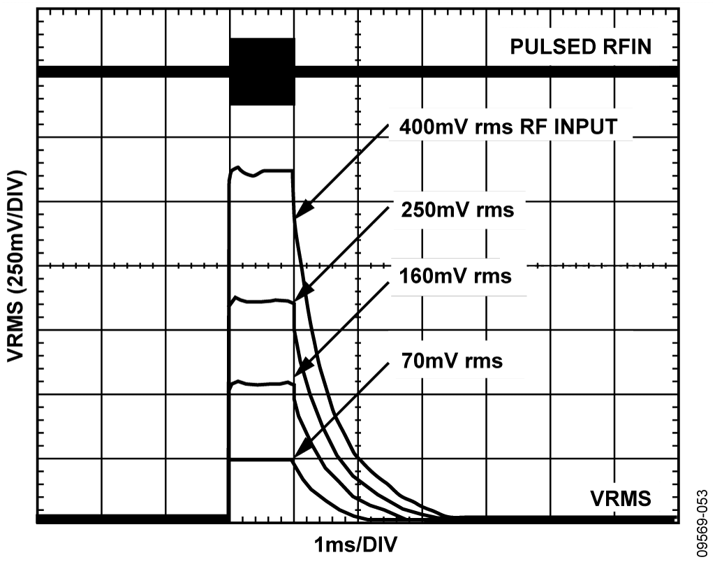
The turn-on time and pulse response is strongly influenced by the size of the square-domain filter (CFLTR) and output shunt capacitor connected to the VRMS output. Figure 6 (taken from the ADL5502 data sheet) shows a plot of the output response to an RF pulse on the RFIN pin, with a 0.1 μF output filter capacitor and no square-domain filter capacitor (CFLTR). The falling edge is particularly dependent on the output shunt capacitance.

To improve the falling edge of the enable and pulse responses, a resistor can be placed in parallel with the output shunt capacitor. The added resistance helps to discharge the output filter capacitor. Although this method reduces the power-off time, the added load resistor also attenuates the output (see the Output Drive Capability and Buffering section of the ADL5502 data sheet). Figure 7 (taken from the ADL5502 data sheet) shows the improvement obtained by adding a parallel 1 kΩ resistor.


The RMS and PEAK outputs of the ADL5502 pass through unity gain buffers that drive cross-coupled stages for converting the single-ended outputs to differential signals. The internal +2.5 V reference of the AD7266 (via the DCAPA and DCAPB pins) passes through another unity gain buffer and a voltage divider. This sets the common-mode voltage of the network to +1.25 V.
The AD7266 achieves simultaneous samples of the RMS and PEAK outputs and transfers the data within a 1 μs response time. The data is provided on a single serial data line. Because slope and intercept vary from device to device, board-level calibration must be performed to achieve high accuracy. In general, calibration is performed by applying two input power levels to the ADL5502 and measuring the corresponding output voltages. The calibration points are generally chosen to be within the linear operating range of the device. The best-fit line is characterized by calculating the conversion gain (or slope) and intercept using the following equations:

where:
VIN is the rms input voltage to RFIN.
VVRMS is the voltage output at VRMS.
Once gain and intercept are calculated, an equation can be written that allows calculation of an (unknown) input power based on the measured output voltage.

For an ideal (known) input power, the law conformance error of the measured data can be calculated as

Figure 8 and Figure 9 show plots of the VRMS and PEAK error at 25°C, the temperature at which the ADL5502 is calibrated. Note that the error is not zero; this is because the ADL5502 does not perfectly follow the ideal linear equation, even within its operating region. The error at the calibration points is, however, equal to zero by definition.


When the characteristics (slope and intercept) of the VRMS and PEAK outputs are known, the calibration for the CF calculation is complete. A three-stage process must be taken to measure and calculate the crest factor of any waveform. First, the unknown signal must be applied to the RF input, and the corresponding VRMS level is measured. This level is indicated in Figure 10 as VVRMS-UNKNOWN. The RF input, VIN, is calculated using VVRMS-UNKNOWN and Equation 3.


Next, the CW reference level of PEAK, VPEAK-CW, is calculated using VIN (that is, the output voltage that would be seen if the incoming waveform was a CW signal).

Finally, the actual level of PEAK, VPEAK-UNKNOWN, is measured and the CF can be calculated as

where VPEAK-CW is used as a reference point to compare VPEAK-UNKNOWN. If both VPEAK values are equal, then the CF is 0 dB, as shown in Figure 11 with the CW signal (taken from the ADL5502 data sheet). Across the dynamic range, the calculated CF hovers about the 0 dB line. Likewise, for complex waveforms of 3 dB, 6 dB, and 9 dB CFs, the calculations accurately hover about the corresponding CF levels.


The performance of this or any high speed circuit is highly dependent on proper PCB layout. This includes, but is not limited to, power supply bypassing, controlled impedance lines (where required), component placement, signal routing, and power and ground planes. (See MT-031 Tutorial, MT-101 Tutorial, and article, A Practical Guide to High-Speed Printed-Circuit-Board Layout, for more detailed information regarding PCB layout.) A complete design support package for this circuit note can be found at http://www.analog.com/CN0187-DesignSupport.
Common Variations
For applications that require less RF detection range, the AD8363 rms detector can be used. The AD8363 has a detection range of 50 dB and operates at frequencies up to 6 GHz. For non-rms detection applications, the AD8317/AD8318/AD8319 or ADL5513 can be used. These devices offer varying detection ranges and have varying input frequency ranges up to 10 GHz (see CN-0150 for more details).
Circuit Evaluation & Test
This circuit uses the EVAL-CN0187-SDPZ circuit board and the EVAL-SDP-CB1Z System Demonstration Platform (SDP) evaluation board. The two boards have 120-pin mating connectors, allowing for the quick setup and evaluation of the circuit’s performance. The EVAL-CN0187-SDPZ board contains the circuit to be evaluated, as described in this note, and the SDP evaluation board is used with the CN0187 evaluation software to capture the data from the EVAL-CN0187-SDPZ circuit board.
Equipment Needed
- PC with a USB port and Windows® XP or Windows Vista® (32-bit), or Windows® 7 (32-bit)
- EVAL-CN0187-SDPZ circuit evaluation board
- EVAL-SDP-CB1Z SDP evaluation board
- CN0187 evaluation software
- Power supply: +6 V, or +6 V “wall wart”
- RF signal source
- Coaxial RF cable with SMA connectors
Getting Started
Load the evaluation software by placing the CN0187 Evaluation Software disc in the CD drive of the PC. Using "My Computer," locate the drive that contains the evaluation software disc and open the Readme file. Follow the instructions contained in the Readme file for installing and using the evaluation software.
Functional Block Diagram
See Figure 1 of this circuit note for the circuit block diagram, and the “EVAL-CN0187-SDPZ-SCH” pdf file for the circuit schematics. This file is contained in the CN0187 DesignSupport Package.
Setup
Connect the 120-pin connector on the EVAL-CN0187-SDPZ circuit board to the connector marked “CON A” on the EVAL-SDP-CB1Z evaluation (SDP) board. Nylon hardware should be used to firmly secure the two boards, using the holes provided at the ends of the 120-pin connectors. Using an appropriate RF cable, connect the RF signal source to the EVAL-CN0187-SDPZ board via the SMA RF input connector. With power to the supply off, connect a +6 V power supply to the pins marked “+6 V” and “GND” on the board. If available, a +6 V "wall wart" can be connected to the barrel jack connector on the board and used in place of the +6 V power supply. Connect the USB cable supplied with the SDP board to the USB port on the PC. Note: Do not connect the USB cable to the mini USB connector on the SDP board at this time.
Test
Apply power to the +6 V supply (or “wall wart”) connected to EVAL-CN0187-SDPZ circuit board. Launch the evaluation software and connect the USB cable from the PC to the USB mini-connector on the SDP board. The software will be able to communicate to the SDP board if the Analog Devices System Development Platform driver is listed in the Device Manager.
Once USB communications are established, the SDP board can now be used to send, receive, and capture serial data from the EVAL-CN0187-SDPZ board.
The data in this circuit note were generated using a Rohde & Schwarz SMT-03 RF signal source and an Agilent E3631A power supply. The signal source was set to the frequencies indicated in the graphs, and the input power was stepped and data recorded in 1 dB increments.
Information and details regarding how to use the evaluation software for data capture can be found in the CN0187 Evaluation Software Readme file.
Information regarding the SDP board can be found in the SDP User Guide.