
Save time and deliver your solutions faster with ADI’s new suite of precision technology signal chains. Align your applications ranging from Smart Industry to Instrumentation, Electrification to Digital Health, to exactly the right precision technology combinations.
Tailor your signal chain with confidenceADA4255
RECOMMENDED FOR NEW DESIGNSZero Drift, High Voltage, Programmable Gain Instrumentation Amplifier with Charge Pump
- Part Models
- 3
- 1ku List Price
- Starting From $5.05
Part Details
- Integrated bipolar charge pump
- Simplified isolation requirements
- Wide input range on low voltage supplies
- Dedicated output amplifier supplies for ADC protection
- Low power: 83 mW (DVDD = 3 V, VDDCP = 5 V)
- 36 precision gains from 1/16 V/V to 176 V/V
- Robust ±60 V protected 2:1 input multiplexer
- Low input bias current: ±1.5 nA maximum at TA = 25°C
- Integrated input EMI filtering
- 7 GPIOx ports with special functions
- Sequential chip select mode
- Excellent dc precision
- Low input offset voltage: ±14 µV maximum
- Low input offset voltage drift: ±0.08 µV/°C maximum
- Gain calibration via internal memory
- Low gain drift: ±1 ppm/°C maximum
- High CMRR: 111 dB minimum, G = 1 V/V
- Excitation current source
- SPI port with checksum (CRC) support
- Internal/external fault detection
- Compact 28-lead, 5 mm × 5 mm LFCSP
- Specified temperature range: −40°C to +105°C
The ADA4255 is a precision programmable gain instrumentation amplifier (PGIA) with integrated bipolar charge pumps. With its integrated charge pumps, the ADA4255 internally produces the high voltage bipolar supplies needed to achieve a wide input voltage range (38 V typical with VDDCP = 5 V) without lowering input impedance. The charge pump topology of the ADA4255 allows channels to be isolated with only low voltage components, reducing complexity, size, and implementation time in industrial and process control systems.
The zero drift PGIA topology of the ADA4255 self calibrates dc errors and lower frequency 1/f noise, achieving excellent dc precision over the entire specified temperature range. The combination of 36 precision gains ranging from 1/16 V/V to 176 V/V within the ADA4255 and high voltage, high impedance inputs allow a wide range of inputs to be scaled to the range of the analog-to-digital converter (ADC). By integrating all gain setting and level shifting resistors, the ADA4255 achieves excellent common-mode rejection ratio (CMRR) performance (111 dB minimum at G = 1 V/V) and extremely low gain drift (±1 ppm/°C maximum). This high level of precision maximizes dynamic range and greatly reduces calibration requirements in many applications.
The ±60 V input protection, integrated electromagnetic interference (EMI) filtering and various safety features make the ADA4255 an ideal choice for robust industrial systems. Seven general-purpose input and output (GPIOx) pins, which can be configured to provide various special functions, are included in the ADA4255. An excitation current source output is available to bias sensors such as resistance temperature detectors (RTDs).
The ADA4255 is specified over the −40°C to +105°C temperature range and is offered in a compact 5 mm × 5 mm, 28-lead LFCSP.
APPLICATIONS
- Universal process control front ends
- Data acquisition systems
- Test and measurement systems
- System power monitoring
Documentation
Data Sheet 1
User Guide 1
ADI has always placed the highest emphasis on delivering products that meet the maximum levels of quality and reliability. We achieve this by incorporating quality and reliability checks in every scope of product and process design, and in the manufacturing process as well. "Zero defects" for shipped products is always our goal. View our quality and reliability program and certifications for more information.
| Part Model | Pin/Package Drawing | Documentation | CAD Symbols, Footprints, and 3D Models |
|---|---|---|---|
| ADA4255ACPZ | 28-Lead LFSCP (5mm x 5mm x 0.95mm w/ EP) | ||
| ADA4255ACPZ-R7 | 28-Lead LFSCP (5mm x 5mm x 0.95mm w/ EP) | ||
| ADA4255ACPZ-RL | 28-Lead LFSCP (5mm x 5mm x 0.95mm w/ EP) |
This is the most up-to-date revision of the Data Sheet.
Software Resources
Can't find the software or driver you need?
Request a Driver/SoftwareHardware Ecosystem
| Parts | Product Life Cycle | Description |
|---|---|---|
| Fully Differential Amplifiers 2 | ||
| ADA4945-1 | RECOMMENDED FOR NEW DESIGNS | High Speed, ±0.1 µV/˚C Offset Drift, Fully Differential ADC Driver |
| LTC6363 | LAST TIME BUY | Precision, Low Power Differential Amplifier/ADC Driver Family |
| isoPower 4 | ||
| ADuM6420A | RECOMMENDED FOR NEW DESIGNS | Quad-Channel Isolators with Integrated DC-to-DC Converter (4:0 directionality) |
| ADUM6421A | RECOMMENDED FOR NEW DESIGNS | Quad-Channel Isolators with Integrated DC-to-DC Converter (3:1 directionality) |
| ADuM6422A | RECOMMENDED FOR NEW DESIGNS | Quad-Channel Isolators with Integrated DC-to-DC Converter (2:2 directionality) |
| ADUM5010 | PRODUCTION | 2.5kV rms Isolated DC/DC Converter |
| Multiplexed A/D Converters 2 | ||
| AD7175-2 | RECOMMENDED FOR NEW DESIGNS | 24-Bit, 250 kSPS, Sigma-Delta ADC with 20 µs Settling and True Rail-to-Rail Buffers |
| AD7124-4 | RECOMMENDED FOR NEW DESIGNS | 4-Channel, Low Noise, Low Power, 24-Bit, Sigma-Delta ADC with PGA and Reference |
| Series Voltage References 3 | ||
| ADR4550 | PRODUCTION | Ultra-Low-Noise, High-Accuracy 5.0V Voltage Reference |
| ADR3450 | PRODUCTION | Micro-Power, High-Accuracy 5.0V Voltage Reference |
| LT6656 | PRODUCTION | 1μA Precision Series Voltage Reference |
| Simultaneous Sampling A/D Converters 1 | ||
| AD7768 | RECOMMENDED FOR NEW DESIGNS | 8-Channel, 24-Bit, Simultaneous Sampling ADC, Power Scaling, 110.8 kHz BW |
| Single Channel A/D Converters 1 | ||
| AD4007 | RECOMMENDED FOR NEW DESIGNS | 18-Bit, 2 MSPS/1 MSPS/500 kSPS, Easy Drive, Differential SAR ADCs |
| Standard Digital Isolators 8 | ||
| ADuM6423A | RECOMMENDED FOR NEW DESIGNS | Quad-Channel Isolators with Integrated DC-to-DC Converter (1:3 directionality) |
| ADUM6424A | RECOMMENDED FOR NEW DESIGNS | Quad-Channel Isolators with Integrated DC-to-DC Converter (0:4 directionality) |
| ADUM140D | RECOMMENDED FOR NEW DESIGNS |
Robust, Quad Channel Isolator W/ Input Disable & 0 Reverse Channels |
| ADUM140E | RECOMMENDED FOR NEW DESIGNS |
Robust, Quad Channel Isolator W/ Output Enable & 0 Reverse Channels |
| ADUM141D | RECOMMENDED FOR NEW DESIGNS |
Robust, Quad Channel Isolator W/ Input Disable & 1 Reverse Channel |
| ADUM141E | RECOMMENDED FOR NEW DESIGNS |
Robust, Quad Channel Isolator W/ Output Enable & 1 Reverse Channel |
| ADUM142D | RECOMMENDED FOR NEW DESIGNS |
Robust, Quad Channel Isolator W/ Input Disable & 2 Reverse Channels |
| ADUM142E | RECOMMENDED FOR NEW DESIGNS |
Robust, Quad Channel Isolator W/ Output Enable & 2 Reverse Channels |
Tools & Simulations
LTspice
Models for the following parts are available in LTspice:
- ADA4255
In-Amp Diamond Plot Tool
The Diamond Plot Tool is a web application that generates a configuration-specific Output Voltage Range vs. Input Common-Mode Voltage graph, also known as the Diamond Plot, for Analog Devices Instrumentation Amplifiers. Based on user inputs such as supply voltage, gain, and input signal range, the tool detects saturation and recommends in-amps for which the input signal is in-range and the configuration is valid. Avoid saturation, find the best in-amp for your design, and save time.
Open ToolSignal Chain Designer
Signal Chain Designer is a web-based tool designed to create and simulate complex precision signal chains. See your circuit’s performance before you commit to your PCB: transfer function, noise, power consumption, input range, and DC error. Quickly experiment with different parts and architectures. Signal chains can be exported to LTspice for further analysis.
Open ToolIBIS Model 1
SPICE Model 1
LTspice® is a powerful, fast and free simulation software, schematic capture and waveform viewer with enhancements and models for improving the simulation of analog circuits.
Evaluation Kits
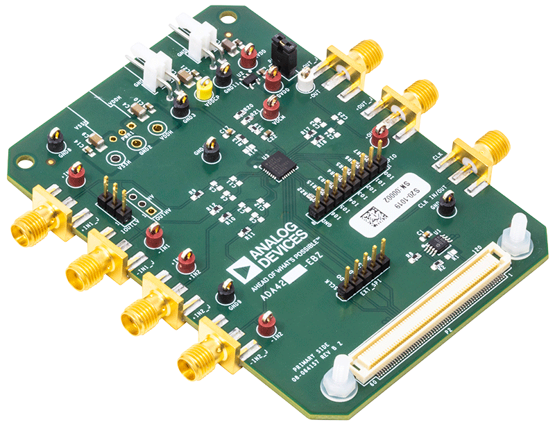


Evaluating the ADA4255 Zero Drift, High Voltage, Programmable Gain Instrumentation Amplifier with Charge Pump