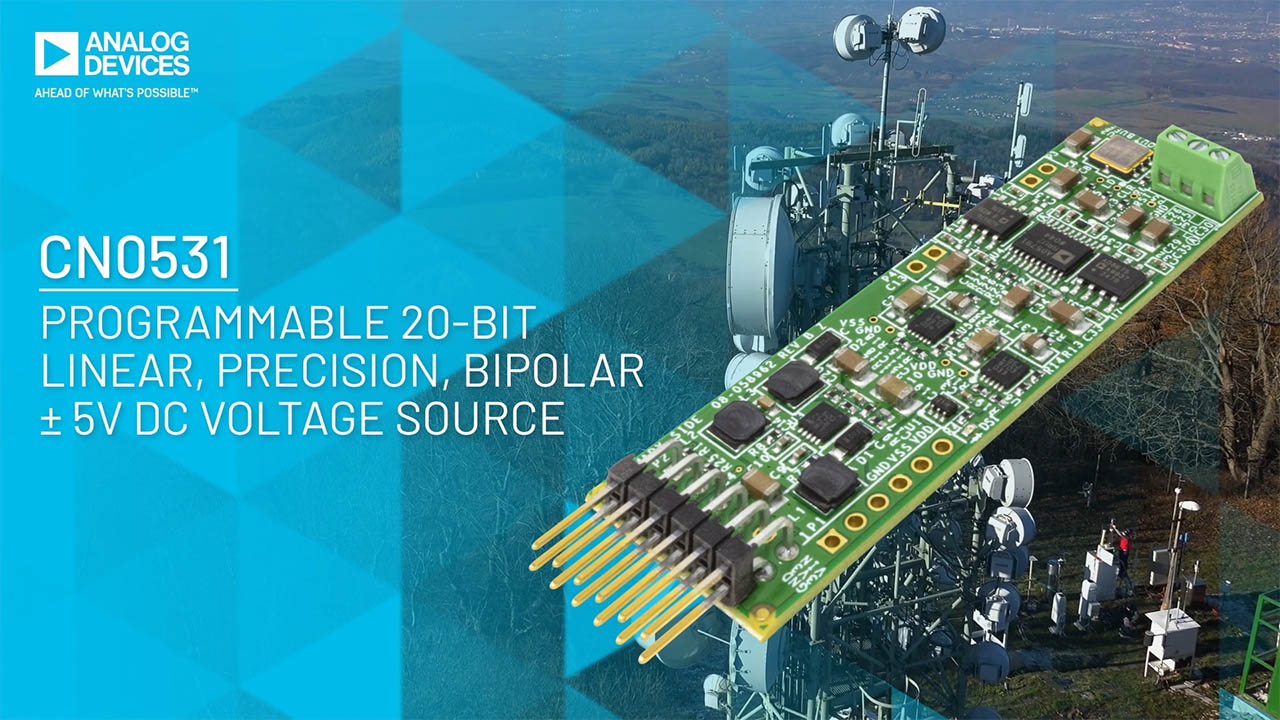
CN0531


Overview
Design Resources
Design & Integration File
- Schematic
- Bill of Materials
- Gerber Files
- Layout Files
- Assembly Drawings
- Allegro Board File
Evaluation Hardware
Part Numbers with "Z" indicate RoHS Compliance. Boards checked are needed to evaluate this circuit.
- EVAL-ADICUP3029 ($52.97) Ultralow Power Arduino Form Factor Compatible Development Platform
- EVAL-CN0531-PMDZ ($175.37) 20-bit Digital to Analog Converter System
Device Drivers
Software such as C code and/or FPGA code, used to communicate with component's digital interface.
AD576x, AD578x, AD579x GitHub no-OS Driver Source Code
AD5760, AD578x, AD579x IIO DAC GitHub Linux Driver Source Code
Features & Benefits
- +/-5V Output Range
- 20-Bit Signal Generation Control
- On board precision 5V Reference
- All Power Rails Generated Using a Single 3.3V Source
Markets and Technologies
Parts Used
Documentation & Resources
-
CN0531 User Guide3/5/2021WIKI
-
Solutions For Rapid Prototyping: Answering the Needs of Practicing Engineers8/23/2023PDF784 K

Circuit Function & Benefits
Precision dc voltages are a critical component of scientific instrumentation and measurement equipment, automated test equipment, factory automation and control, chemical analysis, and many other high precision applications. The most demanding applications require single digit, part per million temperature drift, subppm linearity, and low, predictable noise performance.
The circuit shown in Figure 1 is a programmable 20-bit voltage source that enables these demanding applications. The output range is −5 V to +5 V with ±1 LSB integral nonlinearity (INL), ±1 LSB differential nonlinearity (DNL), and exceptionally low noise and low drift across the entire output range.
On-board power converters produce the required supply rails from a single voltage supply provided by the development platform board. Low noise, high power supply rejection ratio (PSRR) voltage regulators ensure that the switching noise is minimized. A high precision, high stability, on-board hermetically sealed voltage reference ensures the high precision and accuracy of the 20-bit system.
The output of the circuit is a buffered voltage with an option for a remote sense connection to compensate for lead resistance or allow for the insertion of an external power stage, if necessary, providing drive flexibility for the desired end application.


Circuit Description
Digital to Analog Conversation
The core of the circuit shown in Figure 1 is the AD5791, a 20-bit digital-to-analog converter (DAC) with a serial peripheral interface (SPI), offering ±1 LSB INL and ±1 LSB DNL performance and 7.5 nV/√Hz noise spectral density. The AD5791 also exhibits an extremely low temperature drift of 0.05 ppm/°C. The precision architecture of the AD5791 requires force sense buffering of its voltage reference inputs to ensure specified linearity.
The amplifiers chosen to buffer the reference inputs must have low noise, low temperature drift, and low input bias currents. The recommended amplifier for this function is the AD8676, an ultraprecision, 36 V, 2.8 nV/√Hz, dual op amp, exhibiting a low offset drift of 0.6 µV/°C and an input bias current of 2 nA. In addition, the AD5791 is characterized and factory calibrated using this dual op amp to buffer its voltage reference inputs, further enhancing confidence in this combination of components.
The circuit can be software configurated in two modes, bipolar or unipolar. Figure 1 shows the bipolar configuration in which the output voltage ranges between −5 V to +5 V by using a single 5 V reference buffered by the AD8676. To determine the output voltage in bipolar mode, use the following equation:

where:
VOUT is the output voltage.
VREF is the reference voltage (5 V on CN-0531).
Code is the 20-bit code programmed into the DAC.
When configured in unipolar mode, R1 is internally connected in parallel with RFB, and the output range is 0 V to 5 V (see Figure 1). To determine the output voltage in unipolar mode, use the following equation:

Voltage Reference
A programmable voltage source is only as good as its voltage reference, which determines the output span of the source. The extremely small 0.05 ppm/°C gain drift of the AD5791 results in the voltage reference becoming a limiting factor for gain accuracy and drift in most applications.
The LTC6655BHLS8-5 provides a highly stable and accurate 5.0 V reference for the CN0531. This reference has an initial accuracy of 0.025% with 2 ppm/°C maximum temperature drift, and 0.25 ppm noise (0.1 Hz to 10 Hz). The hermetic package is insensitive to humidity and provides an outstanding thermal hysteresis of 30 ppm.
Long-term drift is exceptional, typically 20 ppm/√kHr. Long-term drift cannot be extrapolated from accelerated high temperature testing, which is an erroneous technique that delivers drift numbers that are wildly optimistic. The only way long-term drift is determined is to measure the drift over the time interval of interest, and the LTC6555 has undergone extensive characterization over thousands of hours of operating time. Refer to the LTC6655 data sheet and Design Note 229 for further information on these methods.
The level of performance of the LTC6655 is rivaled only by more exotic and expensive voltage references that employ heaters, closed-loop temperature control, and insulated packaging, thus this device is an optimal combination of performance, power, and cost for the CN0531.
Output Buffer Stage
The AD5791 employs a voltage output, segmented R-2R DAC architecture, which inherently has excellent full-scale and zero-scale error, and the INL and DNL both have a 1 LSB maximum. The output is unbuffered with a constant resistance of 3.4 kΩ, requiring additional signal conditioning in most applications, ideally preserving the dc accuracy and noise specifications of the AD5791.
The AD8675 is a suitable amplifier with an 10 μV typical offset, a 0.6 μV/°C maximum drift, and a 2 nA maximum bias current.
By default, the AD5791 RFB path is connected to the output of the buffer. For applications requiring higher drive capability or remote sense, the on-board connection can be opened and feedback connected remotely at the output of a power buffer stage, for example.
Power Tree
The CN0531 power tree, shown in Figure 2, consists of an LT3471 boost/inverting converter followed by the LT3042 (positive) and the LT3093 (negative) ultralow noise, ultrahigh PSRR linear regulators.
The LT3471 allows the circuit to operate from a single 3.3 V or 5 V supply provided by the development platform board. The output voltages are set to ±8 V, which are then regulated to ±7.5 V by the LT3042 and the LT3093. The LT3042 and the LT3093 provide an exceptional 80 dB and 75 dB PSRR, respectively, at the 1.2 MHz switching frequency of the LT3471, ensuring minimal switching feedthrough at the DAC output.

Figure 2. Simplified Power Block Diagram
CN0531 Linearity Measurements
The following data shown in Figure 3 demonstrates the precision performance of the circuit shown in Figure 1 configured in bipolar mode by using a 6½ digit, Truevolt digital multimeter (DMM). Figure 3 shows the INL of the CN0531 as a function of the DAC code. The results are within the AD5791 data sheet specifications of ±1 LSB.


Noise Calculations and Measurements
The 7.5 nV/√Hz output noise spectral density of the AD5791 is entirely due to its 3.4 kΩ source impedance. The AD8676 output buffer has a voltage noise density of 2.8 nV/√Hz and a current noise density of 0.3 pA/√Hz, producing a negligible 1 nV/√Hz looking into the output resistance of the AD5791. The total noise of the DAC and output amplifier is then

This value is the expected noise when the output is set to 0 V. As the DAC output increases, the noise is dominated by the LTC6655BHLS8-5 reference. Figure 4 shows the output power spectral density for an output voltage of 5.0 V.


Common Variations
The AD5791 can support a wide variety of output ranges from 0 V to ±10 V. The configuration as shown in Figure 1 can be used to generate symmetrical or asymmetrical ranges as required. For the unity-gain mode of operation, set the RBUF bit of the AD5791 internal control register to Logic 1.
The AD5791 also offers a gain of 2 mode of operation that generates a symmetrical bipolar output range from a single positive voltage reference, as described in the AD5791 data sheet, removing the necessity to generate a negative voltage reference. This mode, however, results in larger full-scale and zero-scale errors. To select this mode, set the RBUF bit of the AD5791 internal control register to Logic 0.
Circuit Evaluation & Test
Getting Started
The basic steps and equipment required to test the CN0531 reference design follow. For more information and complete details on the setup instructions, see the CN0531 user guide.
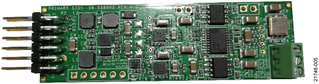
Figure 5. Photograph of the EVAL-CN0531-PMDZ Reference Design Board
Equipment Needed
The following equipment is needed:
- A PC with a USB port
- A serial terminal program, such as Tera Term or PuTTY
- The EVAL-CN0531-PMDZ reference design board
- The EVAL-ADICUP3029 development platform board
- The ADuCM3029_demo_cn0531.hex file
- A microUSB to USB Type A cable
- A 6½ digit or higher, Truevolt DMM
Functional Block Diagram
Figure 6 shows a test setup of the function block diagram of the CN0531.

Figure 6. Test Setup Functional Block Diagram
Test
Use the following steps to test this circuit:
- Connect the EVAL-CN0531-PMDZ to the EVAL-ADICUP3029 using the P8 connector (see Figure 7).
- Connect a DMM to the EVAL-CN0531-PMDZ.
- Plug the USB Type A connector into the PC and the microUSB connector into the EVAL-ADICUP3029.
- Flash the EVAL-ADICUP3029 with the aducm3029_CN0531_demo.hex firmware.
- Press the 3029_Reset button on the EVAL-ADICUP3029.
- Open a serial terminal connecting the EVAL-ADICUP3029 to the PC and type the help command.
- Using the serial terminal, configure the CN0531 into unipolar and set the output voltage to 2.5 V. The serial terminal should look something like Figure 8.
- Verify that the output voltage set in the serial terminal matches the voltage shown on the DMM in Figure 9.


