LT3062
推荐用于新设计45V VIN、微功率、低噪声、200mA LDO
- 产品模型
- 32
产品详情
- 输入电压范围:1.6V 至 45V
- 输出电流:200mA
- 静态电流:45μA
- 压差电压:300mV
- 低噪声:30μVRMS (10Hz 至 100kHz)
- 可调输出 (VREF = 600mV)
- 固定输出电压:3.3V、5V
- 输出容差:±2% (在整个负载、电压和温度范围内)
- 单个电容器用于实现软起动基准并降低输出噪声
- 停机电流:< 1μA
- 反向电池保护
- 电流限制折返和热限制保护
- 8 引脚 2mm x 3mm DFN 封装和 MSOP 封装
LT®3062 是一款微功率、低压差 (LDO) 线性稳压器,其工作在一个 1.6V 至 45V 的电源范围,并可提供一系列的固定输出和可调版本。该器件可提供 200mA 的输出电流和一个 300mV 的典型压差电压。单个外部电容器提供了可编程低噪声基准性能和输出软起动功能。LT3062 的静态电流仅为 45μA,并利用一个最小 3.3μF 的输出电容器实现了快速瞬态响应。在停机模式中,静态电流小于 1μA,而且基准软起动电容器复位。
LT3062 利用低 ESR 陶瓷输出电容器优化了稳定性和瞬态响应。LT3062 不像其他稳压器所常见的那样需要额外的 ESR。
内部保护电路包括反向电池保护、反射输出保护、反向电流保护、具折返的电流限制和热停机。
LT3062 可提供 3.3V 和 5V 的固定输出电压,可以用作一款具有一个从 600mV 基准至高达 40V 输出电压范围的可调型器件。LT3062 采用耐热性能增强型 8 引脚 2mm x 3mm DFN 封装和 MSOP 封装。
Applications
- 电池供电型系统
- 汽车电源
- 工业电源
- 航空电子设备电源
- 便携式仪器
参考资料
数据手册 1
可靠性数据 1
用户手册 1
技术文章 2
解决方案设计及宣传手册 1
新闻 1
模拟对话 1
ADI 始终高度重视提供符合最高质量和可靠性水平的产品。我们通过将质量和可靠性检查纳入产品和工艺设计的各个范围以及制造过程来实现这一目标。出货产品的“零缺陷”始终是我们的目标。查看我们的质量和可靠性计划和认证以了解更多信息。
| 产品型号 | 产品生命周期 | PCN |
|---|---|---|
|
2月 3, 2020 - 20_0128 Laser Top Mark for 8 Lead MSOP Packages Assembled in ADPG and UTAC |
||
| LT3062EMS8E#PBF | 量产 | |
| LT3062EMS8E#TRPBF | 量产 | |
| LT3062EMS8E-3.3#PBF | 量产 | |
| LT3062EMS8E-3.3#TRPBF | 量产 | |
| LT3062EMS8E-5#PBF | 量产 | |
| LT3062EMS8E-5#TRPBF | 量产 | |
| LT3062HMS8E#PBF | 量产 | |
| LT3062HMS8E#TRPBF | 量产 | |
| LT3062IMS8E#PBF | 量产 | |
| LT3062IMS8E#TRPBF | 量产 | |
| LT3062IMS8E-3.3#PBF | 量产 | |
| LT3062IMS8E-3.3#TRPBF | 量产 | |
| LT3062IMS8E-5#PBF | 量产 | |
| LT3062IMS8E-5#TRPBF | 量产 | |
| LT3062MPMS8E#PBF | 量产 | |
| LT3062MPMS8E#TRPBF | 量产 | |
这是最新版本的数据手册
软件资源
找不到您所需的软件或驱动?
申请驱动/软件硬件生态系统
工具及仿真模型
LTspice 1
LTspice中提供以下器件型号:
- LT3062
LTspice®是一款强大高效的免费仿真软件、原理图采集和波形观测器,为改善模拟电路的仿真提供增强功能和模型。
评估套件


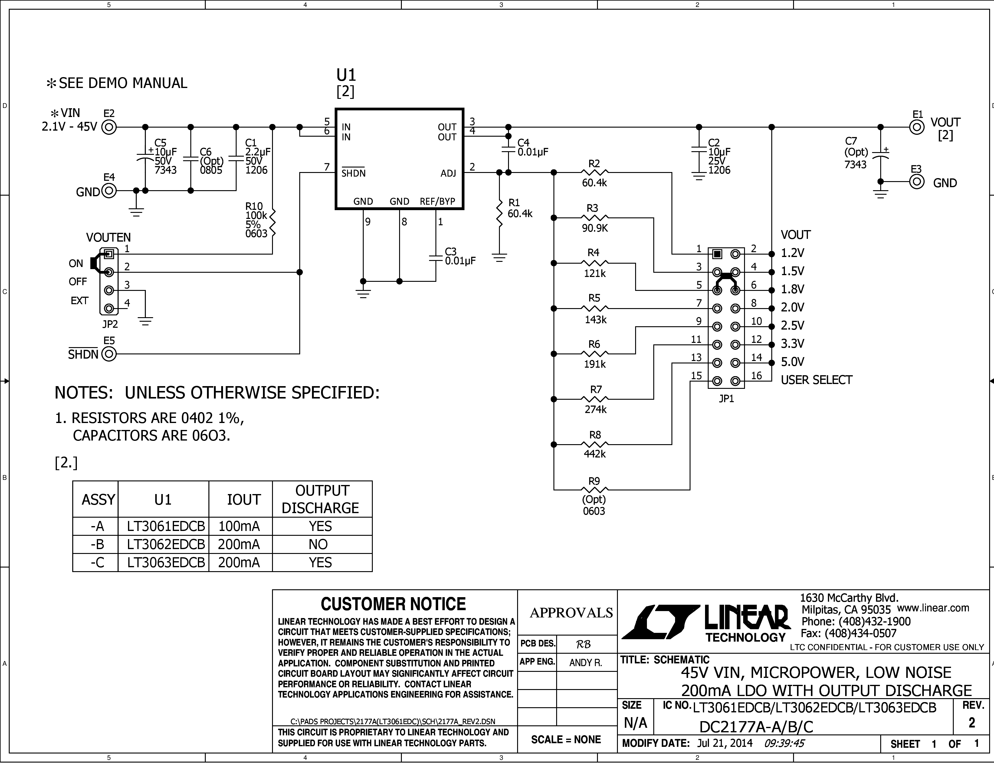
LT3062演示板 | 微功耗、低噪声LDO,2.1V ≤ VIN ≤ 45V,VOUT = 1.2V至5V (200mA)
资料
参考电路


最新评论
需要发起讨论吗? 没有关于 LT3062的相关讨论?是否需要发起讨论?
在EngineerZone®上发起讨论