LTC3315B
推荐新设计使用双通道、5V、2A同步降压型DC/DC转换器,采用2mm x 2mm LQFN封装
- 产品模型
- 18
产品详情
- 双输出,每个输出的输出电流为 2A
- 高效率:19mΩ NMOS 和 75mΩ PMOS
- 宽带宽,快速瞬态响应
- 开关频率可同步至高达 10MHz
- VIN 范围:2.25V 至 5.5V
- VOUT 范围:0.5V 至 VIN
- VOUT 精度:±1%
- 低纹波 Burst Mode® 运行
- 峰值电流模式控制
- 最短接通时间:25ns
- 安全承受过载电感饱和
- 关断电流:1.2µA
- 精密 400mV 启用阈值
- 内部软启动和补偿
- 电源正常输出
- 纤薄耐热性能增强型 12 引脚
2mm × 2mm × 0.74mm LQFN 封装 - 符合汽车应用的 AEC-Q100 标准
LTC3315B具有双2A单片同步降压型转换器,这些转换器依靠2.25V至5.5V输入电源运行,并且采用的封装适用于空间受限并具有苛刻性能要求的应用。两个降压转换器在高达10MHz的开关频率下使用恒定频率峰值电流模式控制,最小接通时间低至25ns,可在小尺寸的应用封装中实现高效率和快速瞬态响应。
LTC3315B可在强制连续或脉冲跳跃模式下工作以实现低噪声,或在Burst Mode®下工作以在轻负载条件时实现高效率。常用的降压开关频率为6MHz,并可通过MODE/SYNC引脚与外部振荡器同步。
LTC3315B可以调节低至500mV的输出。其他特性包括精密启用阈值、PGOOD信号、输出过压保护、热关断、输出短路保护和高达100%占空比的低压差操作。LTC3315B采用紧凑的2mm × 2mm LQFN封装。
应用
- 服务器、电信电源、光学网络
- 分布式直流电源系统(POL)
- FPGA、ASIC、微处理器内核电源
- 工业/汽车/通信
参考资料
数据手册 1
可靠性数据 1
ADI 始终高度重视提供符合最高质量和可靠性水平的产品。我们通过将质量和可靠性检查纳入产品和工艺设计的各个范围以及制造过程来实现这一目标。出货产品的“零缺陷”始终是我们的目标。查看我们的质量和可靠性计划和认证以了解更多信息。
| 产品型号 | 引脚/封装图-中文版 | 文档 | CAD 符号,脚注和 3D模型 |
|---|---|---|---|
| LTC3315BEV#TRMPBF | 12-Lead LQFN (2mm x 2mm x 0.74mm) | ||
| LTC3315BEV#TRPBF | 12-Lead LQFN (2mm x 2mm x 0.74mm) | ||
| LTC3315BEV#WTRMPBF | 12-Lead LQFN (2mm x 2mm x 0.74mm) | ||
| LTC3315BEV#WTRPBF | 12-Lead LQFN (2mm x 2mm x 0.74mm) | ||
| LTC3315BHV#TRMPBF | 12-Lead LQFN (2mm x 2mm x 0.74mm) | ||
| LTC3315BHV#TRPBF | 12-Lead LQFN (2mm x 2mm x 0.74mm) | ||
| LTC3315BHV#WTRMPBF | 12-Lead LQFN (2mm x 2mm x 0.74mm) | ||
| LTC3315BHV#WTRPBF | 12-Lead LQFN (2mm x 2mm x 0.74mm) | ||
| LTC3315BIV#TRMPBF | 12-Lead LQFN (2mm x 2mm x 0.74mm) | ||
| LTC3315BIV#TRPBF | 12-Lead LQFN (2mm x 2mm x 0.74mm) | ||
| LTC3315BIV#WTRMPBF | 12-Lead LQFN (2mm x 2mm x 0.74mm) | ||
| LTC3315BIV#WTRPBF | 12-Lead LQFN (2mm x 2mm x 0.74mm) | ||
| LTC3315BJV#TRMPBF | 12-Lead LQFN (2mm x 2mm x 0.74mm) | ||
| LTC3315BJV#TRPBF | 12-Lead LQFN (2mm x 2mm x 0.74mm) | ||
| LTC3315BJV#WTRMPBF | 12-Lead LQFN (2mm x 2mm x 0.74mm) | ||
| LTC3315BJV#WTRPBF | 12-Lead LQFN (2mm x 2mm x 0.74mm) | ||
| LTC3315BMPV#TRMPBF | 12-Lead LQFN (2mm x 2mm x 0.74mm) | ||
| LTC3315BMPV#TRPBF | 12-Lead LQFN (2mm x 2mm x 0.74mm) |
这是最新版本的数据手册
工具及仿真模型
LTspice 1
LTspice中提供以下器件型号:
- LTC3315A
- LTC3315B
LTspice®是一款强大高效的免费仿真软件、原理图采集和波形观测器,为改善模拟电路的仿真提供增强功能和模型。
评估套件
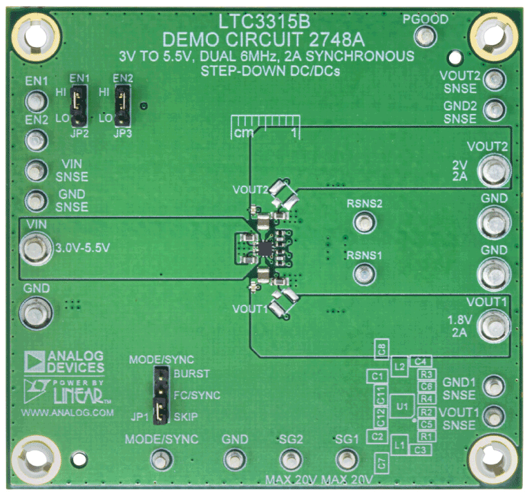
3.3V VIN, Dual 2A, 6MHz Synchronous Step-Down Regulators at 1.8V and 2.0V Outputs, in a 0.71cm2 Solution
资料
最新评论
需要发起讨论吗? 没有关于 ltc3315b的相关讨论?是否需要发起讨论?
在EngineerZone®上发起讨论