ADF4382A
推荐用于新设计适用于高性能转换器时钟应用的 2.87GHz 至 21GHz 小数 N PLL/VCO
适用于高性能转换器时钟应用的 2.87GHz 至 21GHz 小数 N PLL/VCO
- 产品模型
- 2
产品详情
- 基波输出频率范围:11.5 GHz 至 21 GHz
- 除以 2 输出频率范围:5.75 GHz 至 10.5 GHz
- 除以 4 输出频率范围:2.875 GHz 至 5.25 GHz
- 20 GHz 时的积分 RMS 抖动 = 20 fs(积分带宽:100 Hz 至 100 MHz)
- 20 GHz 时的积分 RMS 抖动 = 31 fs(ADC SNR 方法)
- VCO 快速校准时间 < 1 μs
- VCO 自动校准时间 < 100 μ秒
- 相位本底噪声:20 GHz 时为 −156 dBc/Hz
- PLL 规格
- −239dBc/Hz:归一化带内相位本底噪声
- −287dBc/Hz:归一化 1/f 相位本底噪声
- 625 MHz 最大相位/频率检测器输入频率
- 4.5 GHz 参考输入频率
- 典型杂散 fPFD:−90 dBc
- 基准输出延迟规格
- 传播延迟温度系数:0.06 ps/°C
- 调整步长:<1ps
- 多芯片输出相位对齐
- 3.3V 和 5V 电源
- 支持 ADIsimPLL™ 环路滤波器设计工具
- 7 mm × 7 mm、48 端子 LGA
- 工作温度 −40°C 至 105°C
ADF4382A 是一款高性能、超低抖动、小数 N 分频锁相环 (PLL),带有集成电压控制振荡器 (VCO),非常适合 5G 应用或数据转换器时钟应用的本地振荡器 (LO) 生成。高性能 PLL 具有 −239dBc/Hz、低 1/f 噪声和整数模式下 625 MHz 的高 PFD 频率,可实现超低带内噪声和集成抖动性能。ADF4382A 可产生 11.5 GHz 至 21 GHz 基本倍频范围内的频率,从而无需使用次谐波滤波器。ADF4382A 上的 2 分频和 4 分频输出分频器可分别产生 5.75 GHz 至 10.5 GHz 和 2.875 GHz 至 5.25 GHz 的频率。
对于多数据转换器时钟应用,ADF4382A 通过在 PLL 反馈环路中包含输出分频器,自动将其输出与输入参考边沿对齐。对于需要确定性延迟或延迟调整功能的应用,提供分辨率 <1ps 的可编程输出延迟参考。通过参考跨多个设备和整个温度的输出延迟匹配,可以实现可预测且精确的多芯片对齐。
ADF4382A 框图十分简洁,具有简化的串行外设接口 (SPI) 寄存器映射、外部 SYNC 输入以及整数和小数模式下可重复的多芯片对齐,从而缩短了开发时间。
应用
- 高性能数据转换器时钟
- 无线基础设施(MC-GSM、5G、6G)
- 测试和测量
参考资料
数据手册 1
应用笔记 1
视频 1

器件驱动器 3
ADI 始终高度重视提供符合最高质量和可靠性水平的产品。我们通过将质量和可靠性检查纳入产品和工艺设计的各个范围以及制造过程来实现这一目标。出货产品的“零缺陷”始终是我们的目标。查看我们的质量和可靠性计划和认证以了解更多信息。
| 产品型号 | 引脚/封装图-中文版 | 文档 | CAD 符号,脚注和 3D模型 |
|---|---|---|---|
| ADF4382ABCCZ | 48-Terminal Land Grid Array [LGA] (7mm x 7mm x 1.25 mm) | ||
| ADF4382ABCCZ-RL7 | 48-Terminal Land Grid Array [LGA] (7mm x 7mm x 1.25 mm) |
这是最新版本的数据手册
软件资源
器件驱动器 3
Evaluation Software 0
找不到您所需的软件或驱动?
工具及仿真模型
ADIsimPLL™
ADIsimPLL可以对ADI公司最新的高性能PLL产品进行快速、可靠的评估。它是目前最全面的PLL频率合成器设计和仿真工具,可实现所有对PLL性能有显著影响的重要非线性效应仿真。ADIsimPLL可以免去设计过程中的至少一项重复劳动,从而加快上市速度。
打开工具IBIS 模型 1
LTspice®是一款强大高效的免费仿真软件、原理图采集和波形观测器,为改善模拟电路的仿真提供增强功能和模型。
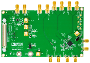
评估套件