ADE9112
推荐新设计使用Isolated, Sigma-Delta ADCs with SPI
- 产品模型
- 2
产品详情
- 2 (ADE9112) or 3 (ADE9113) channel isolated, simultaneously sampling Σ-Δ ADCs, with integrated isoPower, isolated dc-to-dc converters
- 3 (ADE9103) channel nonisolated, simultaneously sampling Σ-Δ ADCs
- Synchronization of multiple ADE9103/ADE9112/ADE9113 devices
- 4-wire SPI with bidirectional CRC and daisy-chain functionality
- Unique SPI readable part ID registers
- Up to 4 ADE9103/ADE9112/ADE9113 devices clocked from a single crystal or an external clock
- IRQ hardware pin and registers for fault detection and robustness
- Sample rate up to 32 kSPS
- SNR up to 95 dB
- ±31.25 mV peak analog input voltage range for current channel
- ±500 mV peak single-ended analog input voltage range for voltage channels
- Internal voltage reference temperature coefficient: <13 ppm/°C typical
- ADC offset drift: <2 nV/°C typical
- Ideal for both AC and DC measurement systems
- Single 3.3 V supply for isolated and nonisolated measurements
- Compact 28-lead, wide-body with finer pitch SOIC package with 8.3 mm creepage
- Temperature range: −40°C to +125°C
- Passes CISPR 32 Class B RF Emissions
- ADE9112 and ADE9113 safety and regulatory approvals
- IEC 60747-17 certificate of conformity expected
- 5000 V RMS for 1 minute per UL 1577
- IEC 61010-1 and IEC 62368-1
The ADE9103/ADE9112/ADE9113are precision simultaneously sampling Σ-Δ analog-to-digital converters (ADCs) for both DC and polyphase shunt-based energy metering applications. The ADE9113 integrates safety certified signal and power galvanic isolation with three simultaneously sampling fully differential 24-bit Σ-Δ ADC channels. The ADE9112 features two fully differential Σ-Δ ADC channels for isolated applications where only a single voltage channel is required. The ADE9103 is a nonisolated, 3-channel Σ-Δ ADC for use in applications where isolation is not required, such as for neutral measurement. The ADE9103/ADE9112/ADE9113 all include a high-gain, current channel best suited for use with a shunt resistor as the current sensor. Multiple ADE9103/ADE9112/ ADE9113 devices can be synchronized to sample simultaneously and provide coherent outputs.
The current channel ADC provides an 86 dBFS signal-to-noise ratio (SNR), at a sample rate of 4 kSPS, over a 1.65 kHz signal bandwidth and a typical gain drift of 13 ppm/°C, which enables down to Class 0.2 accuracy. The voltage ADCs provide an SNR of 91 dBFS over the same sample rate and bandwidth. The high gain on the current channel (IP and IM) aids the use of lower resistance shunts for reduced losses due to heat. The low offset drift of 2 nV/°C offers the performance required for DC metering.
The ADE9103/ADE9112/ADE9113 delivers system cost savings and increased robustness. The main ADE9103/ADE9112/ADE9113 can drive clocks of up to three additional ADE9103/ADE9112/ ADE9113 with a single crystal. The bidirectional, serial port interface (SPI) supports a daisy-chain capability, allowing access to all registers while reducing the required microcontroller pin count. The 28-lead SOIC_W_FP allows more compact layouts. Valid data transfers are ensured with bidirectional, cyclic redundancy check (CRC) and IRQ pin alerts the system of critical faults. The ADE9112 and ADE9113 pass CISPR 32 Class B emissions on a 2-layer printed circuit board (PCB) with the addition of a high voltage capacitor and on a 4-layer PCB with an internal stitching capacitor.
APPLICATIONS
- Shunt-based polyphase meters
- Electric vehicle supply equipment
- DC meters
- Power quality monitoring
- Solar inverters
- Process monitoring
- Protective devices
- Isolated sensor interfaces
参考资料
数据手册 1
用户手册 1
技术文章 1
安全和法规认证 1
视频 1

安全和法规认证 1
器件驱动器 1
ADI 始终高度重视提供符合最高质量和可靠性水平的产品。我们通过将质量和可靠性检查纳入产品和工艺设计的各个范围以及制造过程来实现这一目标。出货产品的“零缺陷”始终是我们的目标。查看我们的质量和可靠性计划和认证以了解更多信息。
| 产品型号 | 引脚/封装图-中文版 | 文档 | CAD 符号,脚注和 3D模型 |
|---|---|---|---|
| ADE9112ARNZ | 28-Lead SOIC (Wide, Finer Pitch) | ||
| ADE9112ARNZ-REEL | SM OUTLINE,300ML,25MLPITCH |
这是最新版本的数据手册
软件资源
Evaluation Software 0
找不到您所需的软件或驱动?
硬件生态系统
| 部分模型 | 产品周期 | 描述 |
|---|---|---|
| 内部电源开关降压稳压器 2 | ||
| MAX17554 | 量产 | 集成60V、50mA、超小型、高效率、同步降压DC-DC转换器 |
| MAX17555 | 推荐新设计使用 | 集成60V、50mA、超小型、高效率、同步降压DC-DC转换器 |
| 微功耗降压稳压器 1 | ||
|
LT8604/ LT8604C |
高效42V/120mA同步降压 | |
| 正线性稳压器(LDO) 3 | ||
| ADP150 | 量产 | 超低噪声、150 mA CMOS线性调节器 |
| ADP7112 | 推荐新设计使用 | 20 V、200 mA低噪声CMOS LDO线性稳压器 |
| ADP7118 | 推荐新设计使用 | 20 V、200 mA、低噪声、CMOS LDO线性稳压器 |
| 部分模型 | 产品周期 | 描述 |
|---|---|---|
| ADE7912 | 量产 | 内置SPI接口的2通道、隔离式Σ-Δ型ADC |
评估套件


AD-ACEVSE22KWZ-KIT
资料
软件

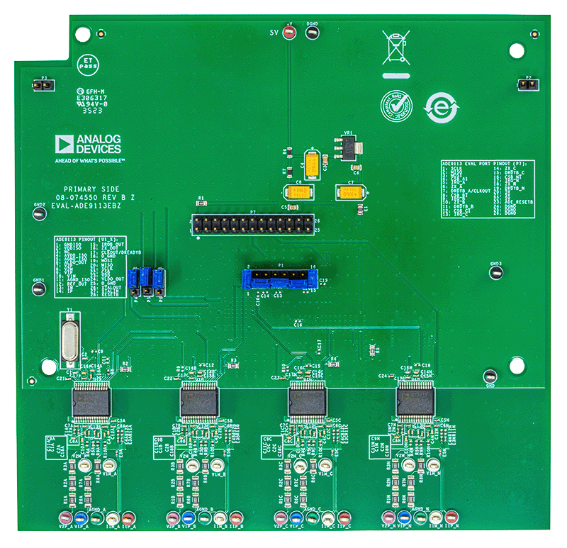
ADE9113(具有SPI接口的隔离式 Σ-Δ ADC)的评估板
资料


Type 2 EVSE 3.6 kW Charging Cable
资料
软件
最新评论
需要发起讨论吗? 没有关于 ADE9112的相关讨论?是否需要发起讨论?
在EngineerZone®上发起讨论